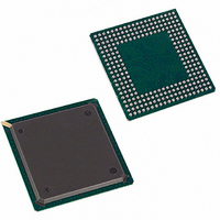
DS3112+W Maxim Integrated Products, DS3112+W Datasheet - Page 91

DS3112+W
Manufacturer Part Number
DS3112+W
Description
IC MUX T3/E3 3.3V 256-PBGA
Manufacturer
Maxim Integrated Products
Datasheet
1.DS3112.pdf
(133 pages)
Specifications of DS3112+W
Controller Type
Framer, Multiplexer
Interface
Parallel/Serial
Voltage - Supply
3.135 V ~ 3.465 V
Current - Supply
150mA
Operating Temperature
0°C ~ 70°C
Mounting Type
Surface Mount
Package / Case
256-PBGA
Lead Free Status / RoHS Status
Lead free / RoHS Compliant
- Current page: 91 of 133
- Download datasheet (3Mb)
Register Name:
Register Description:
Register Address:
Bit #
Name
Default
Bit #
Name
Default
Note 1: When the CPU bus is operated in the 8-bit mode (CMS = 1), the host should always write to the lower byte (bits 0 to 7) first followed
by the upper byte (bits 8 to 15).
Note 2: The THDLC is a write-only register.
Note 3: The Transmit FIFO can be filled to a maximum capacity of 256 bytes. When the Transmit FIFO is full, it will not accept any
additional data.
Bits 0 to 7: Transmit FIFO Data (D0 to D7). Data for the Transmit FIFO can be written to these bits. D0 is the
LSB and is transmitted first while D7 is the MSB and is transmitted last.
Bit 8: Transmit Message End (TMEND). This bit is used to delineate multiple messages in the Transmit FIFO. It
should be set to a one when the last byte of a packet is written to the Transmit FIFO. The setting of this bit
indicates to the HDLC controller that the message is complete and that it should calculate and add in the CRC
checksum and at least two flags. This bit should be set to zero for all other data written to the FIFO. All HDLC
messages must be at least 2 bytes in length.
9.3 HDLC Status and Interrupt Register Description
Register Name:
Register Description:
Register Address:
Bit #
Name
Default
Bit #
Name
Default
Note: See
bits are read-write.
Bit 0: Transmit Packet End (TEND). This latched read-only event-status bit will be set to a one each time the
transmit HDLC controller reads a transmit FIFO byte with the corresponding TMEND bit set or if a FIFO underrun
occurs. This bit will be cleared when read and will not be set again until another message end is detected. The
setting of this bit can cause a hardware interrupt to occur if the TEND bit in the Interrupt Mask for HSR (IHSR)
register is set to a one and the HDLC bit in the Interrupt Mask for MSR (IMSR) register is set to a one. The
interrupt will be allowed to clear when this bit is read.
Bit 2: Transmit FIFO Low Watermark (TLWM). This read-only real time status bit will be set to a one when
the transmit FIFO contains less than the number of bytes configured by the Transmit Low Watermark Setting
control bits (TLWMS0 to TLWMS2) in the HDLC Control Register (HCR). This bit will be cleared when the FIFO
fills beyond the low watermark. The setting of this bit can cause a hardware interrupt to occur if the TLWM bit in
the Interrupt Mask for HSR (IHSR) register is set to a one and the HDLC bit in the Interrupt Mask for MSR
(IMSR) register is set to a one.
Figure 9-1
TUDR
RABT
D7
15
—
—
—
15
—
7
0
7
for details on the signal flow for the status bits in the HSR register. Bits that are underlined are read-only; all other
REMPTY
RPE
D6
14
—
—
—
14
—
6
0
6
THDLC
Transmit HDLC FIFO
84h
HSR
HDLC Status Register
86h
ROVR
RPS
D5
13
—
—
—
13
—
5
0
5
TEMPTY
RHWM
91 of 133
D4
12
—
—
—
12
—
4
0
4
TFL3
D3
11
—
—
—
—
11
—
3
0
3
TLWM
TFL2
D2
10
—
—
—
10
—
2
0
2
TFL1
D1
—
—
—
—
—
1
0
9
1
9
TMEND
TEND
TFL0
D0
—
—
DS3112
0
0
8
0
0
8
Related parts for DS3112+W
Image
Part Number
Description
Manufacturer
Datasheet
Request
R

Part Number:
Description:
IC MUX TEMPE T3/E3 256-BGA
Manufacturer:
Maxim Integrated Products
Datasheet:

Part Number:
Description:
IC MUX TEMPE T3/E3 256-BGA
Manufacturer:
Maxim Integrated Products
Datasheet:

Part Number:
Description:
IC FRAMER DS3/E3 SNGL 144CSBGA
Manufacturer:
Maxim Integrated Products
Datasheet:

Part Number:
Description:
IC 8CH DS3/3 FRAMER 349-BGA
Manufacturer:
Maxim Integrated Products
Datasheet:

Part Number:
Description:
IC 8CH DS3/3 FRAMER 349-BGA
Manufacturer:
Maxim Integrated Products
Datasheet:

Part Number:
Description:
IC 12CH DS3/3 FRAMER 349-BGA
Manufacturer:
Maxim Integrated Products
Datasheet:

Part Number:
Description:
IC 12CH DS3/3 FRAMER 349-BGA
Manufacturer:
Maxim Integrated Products
Datasheet:

Part Number:
Description:
MAX7528KCWPMaxim Integrated Products [CMOS Dual 8-Bit Buffered Multiplying DACs]
Manufacturer:
Maxim Integrated Products
Datasheet:

Part Number:
Description:
Single +5V, fully integrated, 1.25Gbps laser diode driver.
Manufacturer:
Maxim Integrated Products
Datasheet:

Part Number:
Description:
Single +5V, fully integrated, 155Mbps laser diode driver.
Manufacturer:
Maxim Integrated Products
Datasheet:

Part Number:
Description:
VRD11/VRD10, K8 Rev F 2/3/4-Phase PWM Controllers with Integrated Dual MOSFET Drivers
Manufacturer:
Maxim Integrated Products
Datasheet:

Part Number:
Description:
Highly Integrated Level 2 SMBus Battery Chargers
Manufacturer:
Maxim Integrated Products
Datasheet:

Part Number:
Description:
Current Monitor and Accumulator with Integrated Sense Resistor; ; Temperature Range: -40°C to +85°C
Manufacturer:
Maxim Integrated Products

Part Number:
Description:
TSSOP 14/A°/RS-485 Transceivers with Integrated 100O/120O Termination Resis
Manufacturer:
Maxim Integrated Products

Part Number:
Description:
TSSOP 14/A°/RS-485 Transceivers with Integrated 100O/120O Termination Resis
Manufacturer:
Maxim Integrated Products


