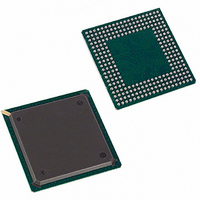
DS3112+W Maxim Integrated Products, DS3112+W Datasheet - Page 35

DS3112+W
Manufacturer Part Number
DS3112+W
Description
IC MUX T3/E3 3.3V 256-PBGA
Manufacturer
Maxim Integrated Products
Datasheet
1.DS3112.pdf
(133 pages)
Specifications of DS3112+W
Controller Type
Framer, Multiplexer
Interface
Parallel/Serial
Voltage - Supply
3.135 V ~ 3.465 V
Current - Supply
150mA
Operating Temperature
0°C ~ 70°C
Mounting Type
Surface Mount
Package / Case
256-PBGA
Lead Free Status / RoHS Status
Lead free / RoHS Compliant
Bit 4: Manual Error Counter Update (MECU). A zero to one transition on this bit will cause the device to
update the performance error counters. This bit is ignored if the AECU control bit is set low. This bit must be
cleared and set again for a subsequent update. This bit is logically ORed with the external FRMECU hardware
input signal. After this bit has toggled, the host must wait at least 100ns before reading the error counters to allow
the device time to complete the update.
Bit 5: High-Speed (T3/E3) Port Unipolar Enable (UNI). When this bit is set low, the device will output a bipolar
coded signal at HTPOS and HTNEG and expect a bipolar coded signal at HRPOS and HRNEG. When this bit is
set high, the device will output a NRZ coded signal at HTPOS and expect a NRZ coded signal at HRPOS. In the
unipolar mode, the device will force the HTNEG output low and the HRNEG input is ignored and should be tied
low. In the unipolar mode, the B3ZS and HDB3 coder/decoders should be disabled by setting the ZCSD bit to one
(ZCSD = 1).
Bit 6: Loss Of Transmit Clock Mux Control (LOTCMC). The DS3112 can detect if the FTCLK fails to
transition. If this bit is set low, the device will take no action (other than setting the LOTC status bit) when the
FTCLK fails to transition. When this bit is set high, the device will automatically switch to the input receive clock
(HRCLK) when the FTCLK fails and transmit AIS.
Bit 7: T3/E3 Transmit Frame Sync I/O Control (FTSOFC). When this bit is set low, the FTSOF signal will be
an output and will pulse for one FTCLK cycle at the beginning of each frame. When this bit is high, the FTSOF
signal is an input and the device uses it to determine the frame boundaries.
Bit 8: Low-Speed (T1/E1) Transmit Port Common Clock Enable (LTCCEN). When this bit is set high, the
LTCLK1 to LTCLK28 and LTCLKA and LTCLKB inputs are ignored and a common clock sourced via the
LTCCLK input is used in their place.
Bit 9: Low-Speed (T1/E1) Receive Port Common Clock Enable (LRCCEN). When this bit is set high, the
LRCLK1 to LRCLK28 and LRCLKA and LRCLKB outputs will all be sourced from the LRCCLK input. This
configuration can only be used in applications where it can be insured that all of the T1 or E1 channels from the far
end are being sourced from a common clock.
Bit 10: High-Speed (T3/E3) Data Enable Mode Select (DENMS). When this bit is set low, the FRDEN and
FTDEN outputs will be asserted during payload data and deasserted during overhead data. When this bit is high,
FRDEN and FTDEN are gapped clocks that pulse during payload data and are suppressed during overhead data.
Bit 11: Low-Speed (T1/E1) Port Loop Timed Mode (LLTM). When this bit is set low, the low-speed T1 and E1
receive clocks (LRCLK) are not routed to the transmit side. When this bit is high, the LRCLKs are routed to the
transmit side to be used as the transmit T1 and E1 clocks. When enabled, all the low-speed ports are looped timed.
This control bit affects all the low-speed ports. The device is not capable of setting individual low-speed ports into
and out of looped timed mode. See the block diagram in
0 = bipolar mode
1 = unipolar mode
0 = do not switch to the HRCLK signal if FTCLK fails to transition
1 = automatically switch to the HRCLK signal if the FTCLK fails to transition and send AIS
0 = FTSOF is an output
1 = FTSOF is an input
0 = disable LTCCLK
1 = enable LTCCLK
0 = disable LRCCLK
1 = enable LRCCLK
0 = FRDEN and FTDEN are data enables
1 = FRDEN and FTDEN are gapped clocks
0 = disable loop timed mode (LRCLK is not used to replace the associated LTCLK)
1 = enable loop timed mode (LRCLK replaces the associated LTCLK)
35 of 133
Figure 1-1
and
Figure 1-2
for more details.
DS3112


