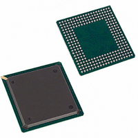
DS3112+W Maxim Integrated Products, DS3112+W Datasheet - Page 15

DS3112+W
Manufacturer Part Number
DS3112+W
Description
IC MUX T3/E3 3.3V 256-PBGA
Manufacturer
Maxim Integrated Products
Datasheet
1.DS3112.pdf
(133 pages)
Specifications of DS3112+W
Controller Type
Framer, Multiplexer
Interface
Parallel/Serial
Voltage - Supply
3.135 V ~ 3.465 V
Current - Supply
150mA
Operating Temperature
0°C ~ 70°C
Mounting Type
Surface Mount
Package / Case
256-PBGA
Lead Free Status / RoHS Status
Lead free / RoHS Compliant
- Current page: 15 of 133
- Download datasheet (3Mb)
PIN
A10
B10
C10
C11
A11
A13
C12
B13
B14
A14
C14
G20
V10
V11
Y13
D5
A3
A9
B9
C9
C8
B8
A7
A8
B6
D7
B5
A4
A5
C6
N2
R1
R3
U2
V2
Y2
Y3
Y5
Y6
V8
V9
CRD(CDS)
LRCLK10
LRCLK11
LRCLK12
LRCLK13
LRCLK14
FRMECU
LRCCLK
LRCLK1
LRCLK2
LRCLK3
LRCLK4
LRCLK5
LRCLK6
LRCLK7
LRCLK8
LRCLK9
HRCLK
HRNEG
HTNEG
FRDEN
HTCLK
(CR/W)
FRCLK
FTCLK
FTDEN
HRPOS
HTPOS
NAME
FRLOF
FRLOS
G.747E
FRSOF
FTMEI
FTSOF
JTCLK
JTRST
JTDO
JTMS
CWR
JTDI
FRD
FTD
TYPE
I/O
O
O
O
O
O
O
O
O
O
O
O
O
O
O
O
O
O
O
O
O
O
O
O
O
O
I
I
I
I
I
I
I
I
I
I
I
I
I
I
I
CPU Bus Read Enable (CPU Bus Data Strobe)
CPU Bus Write Enable (CPU Bus Read/Write Select)
Receive Framer (T3 or E3) Clock Output
Receive Framer (T3 or E3) Data Output
Receive Framer (T3 or E3) Data Enable Output
Receive Framer (T3 or E3) Loss Of Frame Output
Receive Framer (T3 or E3) Loss Of Signal Output
Receive Framer (T3 or E3) Manual Error Counter Update
Receive Framer (T3 or E3) Start Of Frame Pulse
Transmit Framer (T3 or E3) Clock Input
Transmit Framer (T3 or E3) Data Input
Transmit Framer (T3 or E3) Data Enable Output
Transmit Framer (T3 or E3) Manual Error Insert Pulse
Transmit Framer (T3 or E3) Start Of Frame Pulse
G.747 Mode Enable, 0 = Normal T3 Mode, 1 = G.747
Mode
High-Speed (T3 or E3) Port Receive Clock Input
High-Speed (T3 or E3) Port Receive Negative Data Input
High-Speed (T3 or E3) Port Receive Positive or NRZ Data
Input
High-Speed (T3 or E3) Port Transmit Clock Output
High-Speed (T3 or E3) Port Transmit Negative Data
Output
High-Speed (T3 or E3) Port Transmit Positive or NRZ Data
Output
JTAG IEEE 1149.1 Test Serial Clock
JTAG IEEE 1149.1 Test Serial Data Input
JTAG IEEE 1149.1 Test Serial Data Output
JTAG IEEE 1149.1 Test Mode Select
JTAG IEEE 1149.1 Test Reset (Active Low)
Low-Speed (T1 or E1) Port Common Receive Clock Input
Low-Speed (T1 or E1) Receive Clock from Port 1
Low-Speed (T1 or E1) Receive Clock from Port 2
Low-Speed (T1 or E1) Receive Clock from Port 3
Low-Speed (T1 or E1) Receive Clock from Port 4
Low-Speed (T1 or E1) Receive Clock from Port 5
Low-Speed (T1 or E1) Receive Clock from Port 6
Low-Speed (T1 or E1) Receive Clock from Port 7
Low-Speed (T1 or E1) Receive Clock from Port 8
Low-Speed (T1 or E1) Receive Clock from Port 9
Low-Speed (T1 or E1) Receive Clock from Port 10
Low-Speed (T1 or E1) Receive Clock from Port 11
Low-Speed (T1 or E1) Receive Clock from Port 12
Low-Speed (T1 or E1) Receive Clock from Port 13
Low-Speed (T1 or E1) Receive Clock from Port 14
15 of 133
FUNCTION
DS3112
Related parts for DS3112+W
Image
Part Number
Description
Manufacturer
Datasheet
Request
R

Part Number:
Description:
IC MUX TEMPE T3/E3 256-BGA
Manufacturer:
Maxim Integrated Products
Datasheet:

Part Number:
Description:
IC MUX TEMPE T3/E3 256-BGA
Manufacturer:
Maxim Integrated Products
Datasheet:

Part Number:
Description:
IC FRAMER DS3/E3 SNGL 144CSBGA
Manufacturer:
Maxim Integrated Products
Datasheet:

Part Number:
Description:
IC 8CH DS3/3 FRAMER 349-BGA
Manufacturer:
Maxim Integrated Products
Datasheet:

Part Number:
Description:
IC 8CH DS3/3 FRAMER 349-BGA
Manufacturer:
Maxim Integrated Products
Datasheet:

Part Number:
Description:
IC 12CH DS3/3 FRAMER 349-BGA
Manufacturer:
Maxim Integrated Products
Datasheet:

Part Number:
Description:
IC 12CH DS3/3 FRAMER 349-BGA
Manufacturer:
Maxim Integrated Products
Datasheet:

Part Number:
Description:
MAX7528KCWPMaxim Integrated Products [CMOS Dual 8-Bit Buffered Multiplying DACs]
Manufacturer:
Maxim Integrated Products
Datasheet:

Part Number:
Description:
Single +5V, fully integrated, 1.25Gbps laser diode driver.
Manufacturer:
Maxim Integrated Products
Datasheet:

Part Number:
Description:
Single +5V, fully integrated, 155Mbps laser diode driver.
Manufacturer:
Maxim Integrated Products
Datasheet:

Part Number:
Description:
VRD11/VRD10, K8 Rev F 2/3/4-Phase PWM Controllers with Integrated Dual MOSFET Drivers
Manufacturer:
Maxim Integrated Products
Datasheet:

Part Number:
Description:
Highly Integrated Level 2 SMBus Battery Chargers
Manufacturer:
Maxim Integrated Products
Datasheet:

Part Number:
Description:
Current Monitor and Accumulator with Integrated Sense Resistor; ; Temperature Range: -40°C to +85°C
Manufacturer:
Maxim Integrated Products

Part Number:
Description:
TSSOP 14/A°/RS-485 Transceivers with Integrated 100O/120O Termination Resis
Manufacturer:
Maxim Integrated Products

Part Number:
Description:
TSSOP 14/A°/RS-485 Transceivers with Integrated 100O/120O Termination Resis
Manufacturer:
Maxim Integrated Products


