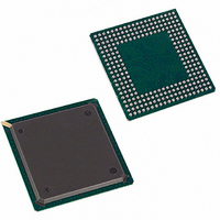
DS3112+W Maxim Integrated Products, DS3112+W Datasheet - Page 36

DS3112+W
Manufacturer Part Number
DS3112+W
Description
IC MUX T3/E3 3.3V 256-PBGA
Manufacturer
Maxim Integrated Products
Datasheet
1.DS3112.pdf
(133 pages)
Specifications of DS3112+W
Controller Type
Framer, Multiplexer
Interface
Parallel/Serial
Voltage - Supply
3.135 V ~ 3.465 V
Current - Supply
150mA
Operating Temperature
0°C ~ 70°C
Mounting Type
Surface Mount
Package / Case
256-PBGA
Lead Free Status / RoHS Status
Lead free / RoHS Compliant
- Current page: 36 of 133
- Download datasheet (3Mb)
Register Name:
Register Description:
Register Address:
Bit #
Name
Default
Bit #
Name
Default
Note: Bits that are underlined are read-only; all other bits are read-write.
Bit 0: HTCLK Invert Enable (HTCLKI).
Bit 1: HTPOS/HTNEG Invert Enable (HTDATI).
Bit 2: HRCLK Invert Enable (HRCLKI).
Bit 3: HRPOS/HRNEG Invert Enable (HTDATI).
Bit 4: HTPOS/HTNEG Force High Disable (HTDATH). Note that this bit must be set by the host in order for
T3/E3 traffic to be output from the device.
Bit 5: HTPOS/HTNEG Force Low Enable (HTDATL).
Bit 8: LTCLK Invert Enable (LTCLKI).
Bit 9: LTDAT Invert Enable (LTDATI).
Bit 10: LRCLK Invert Enable (LRCLKI).
Bit 11: LRDAT Invert Enable (LRDATI).
0 = do not invert the HTCLK signal (normal mode)
1 = invert the HTCLK signal (inverted mode)
0 = do not invert the HTPOS and HTNEG signals (normal mode)
1 = invert the HTPOS and HTNEG signals (inverted mode)
0 = do not invert the HRCLK signal (normal mode)
1 = invert the HRCLK signal (inverted mode)
0 = do not invert the HRPOS and HRNEG signals (normal mode)
1 = invert the HRPOS and HRNEG signals (inverted mode)
0 = force the HTPOS and HTNEG signals high (force high mode)
1 = allow normal transmit data to appear at the HTPOS and HTNEG signals (normal mode)
0 = allow normal transmit data to appear at the HTPOS and HTNEG signals (normal mode)
1 = force the HTPOS and HTNEG signals low (force low mode)
0 = do not invert the LTCLK[n], LTCLKA, LTCLKB, and LTCCLK signals (normal mode)
1 = invert the LTCLK[n], LTCLKA, LTCLKB, and LTCCLK signals (inverted mode)
0 = do not invert the LTDAT[n], LTDATA and LTDATB signals (normal mode)
1 = invert the LTDAT[n], LTDATA and LTDATB signals (inverted mode)
0 = do not invert the LRCLK[n], LRCLKA, LRCLKB, and LRCCLK signals (normal mode)
1 = invert the LRCLK[n], LRCLKA, LRCLKB, and LRCCLK signals (inverted mode)
0 = do not invert the LRDAT[n], LRDATA and LRDATB signals (normal mode)
1 = invert the LRDAT[n], LRDATA and LRDATB signals (inverted mode)
—
—
7
15
—
—
—
—
6
14
—
—
HTDATL
MC2
Master Configuration Register 2
04h
5
0
13
—
—
HTDATH
36 of 133
4
0
12
—
—
HRDATI
LRDATI
11
3
0
0
HRCLKI
LRCLKI
10
2
0
0
HTDATI
LTDATI
1
9
0
0
HTCLKI
LTCLKI
DS3112
0
0
8
0
Related parts for DS3112+W
Image
Part Number
Description
Manufacturer
Datasheet
Request
R

Part Number:
Description:
IC MUX TEMPE T3/E3 256-BGA
Manufacturer:
Maxim Integrated Products
Datasheet:

Part Number:
Description:
IC MUX TEMPE T3/E3 256-BGA
Manufacturer:
Maxim Integrated Products
Datasheet:

Part Number:
Description:
IC FRAMER DS3/E3 SNGL 144CSBGA
Manufacturer:
Maxim Integrated Products
Datasheet:

Part Number:
Description:
IC 8CH DS3/3 FRAMER 349-BGA
Manufacturer:
Maxim Integrated Products
Datasheet:

Part Number:
Description:
IC 8CH DS3/3 FRAMER 349-BGA
Manufacturer:
Maxim Integrated Products
Datasheet:

Part Number:
Description:
IC 12CH DS3/3 FRAMER 349-BGA
Manufacturer:
Maxim Integrated Products
Datasheet:

Part Number:
Description:
IC 12CH DS3/3 FRAMER 349-BGA
Manufacturer:
Maxim Integrated Products
Datasheet:

Part Number:
Description:
MAX7528KCWPMaxim Integrated Products [CMOS Dual 8-Bit Buffered Multiplying DACs]
Manufacturer:
Maxim Integrated Products
Datasheet:

Part Number:
Description:
Single +5V, fully integrated, 1.25Gbps laser diode driver.
Manufacturer:
Maxim Integrated Products
Datasheet:

Part Number:
Description:
Single +5V, fully integrated, 155Mbps laser diode driver.
Manufacturer:
Maxim Integrated Products
Datasheet:

Part Number:
Description:
VRD11/VRD10, K8 Rev F 2/3/4-Phase PWM Controllers with Integrated Dual MOSFET Drivers
Manufacturer:
Maxim Integrated Products
Datasheet:

Part Number:
Description:
Highly Integrated Level 2 SMBus Battery Chargers
Manufacturer:
Maxim Integrated Products
Datasheet:

Part Number:
Description:
Current Monitor and Accumulator with Integrated Sense Resistor; ; Temperature Range: -40°C to +85°C
Manufacturer:
Maxim Integrated Products

Part Number:
Description:
TSSOP 14/A°/RS-485 Transceivers with Integrated 100O/120O Termination Resis
Manufacturer:
Maxim Integrated Products

Part Number:
Description:
TSSOP 14/A°/RS-485 Transceivers with Integrated 100O/120O Termination Resis
Manufacturer:
Maxim Integrated Products


