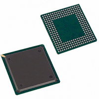
DS3112+W Maxim Integrated Products, DS3112+W Datasheet - Page 49

DS3112+W
Manufacturer Part Number
DS3112+W
Description
IC MUX T3/E3 3.3V 256-PBGA
Manufacturer
Maxim Integrated Products
Datasheet
1.DS3112.pdf
(133 pages)
Specifications of DS3112+W
Controller Type
Framer, Multiplexer
Interface
Parallel/Serial
Voltage - Supply
3.135 V ~ 3.465 V
Current - Supply
150mA
Operating Temperature
0°C ~ 70°C
Mounting Type
Surface Mount
Package / Case
256-PBGA
Lead Free Status / RoHS Status
Lead free / RoHS Compliant
- Current page: 49 of 133
- Download datasheet (3Mb)
5.4 T3/E3 Framer Control Register Description
Register Name:
Register Description:
Register Address:
Bit #
Name
Default
Bit #
Name
Default
Bit 0: T3/E3 Transmit Alarm Indication Signal (TAIS). When this bit is set high in the T3 mode, the transmitter
will generate a properly F-bit and M-bit framed 101010... data pattern with both X bits set to one, all C bits set to
zero, and the proper P bits. This is true regardless of whether the device is in the C-Bit Parity mode or not. When
this bit is set high in the E3 mode, the transmitter will generate an unframed all ones. When this bit it set low,
normal data is transmitted.
Bit 1: T3/E3 Transmit Remote Alarm Indication (TRAI). When this bit is set high in the T3 mode, both X bits
will be set to a zero. When this bit is set high in the E3 mode, the RAI bit (bit number 11 of each E3 frame) will be
set to a one. When this bit it set low in the T3 mode, both X bits will be set to one. When this bit is set low in the
E3 mode, the RAI bit will be set to a zero.
Bit 2: T3/E3 Transmit Pass Through Enable (TPT).
Bits 3 and 4: E3 National Bit Control Bits 0 and 1 (E3SnC0 and E3SnC1). These bits determine from where the
E3 national bit is sourced. On the receive side, the Sn bit is always routed to the T3E3INFO Register as well as the
HDLC controller and the FEAC controller. These bits are ignored in the T3 mode.
Bit 5: Transmit T3 Idle Signal Enable (T3IDLE). When this bit is set high, the T3 Idle Signal will be transmitted
instead of the normal transmit data. The T3 Idle Signal is defined as a normally T3 framed pattern (i.e., with the
proper F bits and M bits along with the proper P bits) where the information bit fields are completely filled with a
data pattern of ...1100... and the C bits in Subframe 3 are set to zero and both X bits are set to one. This bit is
ignored in the E3 mode.
Bit 6: T3/E3 Line Loopback Enable (LLB). See
loopback.
E3SnC1
0
0
1
1
0 = do not transmit AIS
1 = transmit AIS
0 = do not transmit RAI
1 = transmit RAI
0 = enable the framer to insert framing and overhead bits
1 = framer will not insert any framing or overhead bits
0 = transmit data normally
1 = transmit T3 Idle Signal
0 = disable loopback
1 = enable loopback
DLB
15
—
—
7
0
E3SnC0
0
1
0
1
LLB
PLB
6
0
14
0
Force the Sn bit to one
Use the HDLC controller to source the Sn bit
Use the FEAC controller to source the Sn bit
Force the Sn bit to zero
T3E3CR
T3/E3 Control Register
10h
SOURCE OF THE E3 NATIONAL BIT (Sn)
T3IDLE
TFEBE
5
0
13
0
AFEBED
E3SnC1
49 of 133
Figure 1-1
12
0
4
0
and
E3SnC0
ECC
11
0
3
0
Figure 1-2
FECC1
TPT
10
0
2
0
for a visual description of this
FECC0
TRAI
1
0
9
0
E3CVE
TAIS
0
8
0
0
DS3112
Related parts for DS3112+W
Image
Part Number
Description
Manufacturer
Datasheet
Request
R

Part Number:
Description:
IC MUX TEMPE T3/E3 256-BGA
Manufacturer:
Maxim Integrated Products
Datasheet:

Part Number:
Description:
IC MUX TEMPE T3/E3 256-BGA
Manufacturer:
Maxim Integrated Products
Datasheet:

Part Number:
Description:
IC FRAMER DS3/E3 SNGL 144CSBGA
Manufacturer:
Maxim Integrated Products
Datasheet:

Part Number:
Description:
IC 8CH DS3/3 FRAMER 349-BGA
Manufacturer:
Maxim Integrated Products
Datasheet:

Part Number:
Description:
IC 8CH DS3/3 FRAMER 349-BGA
Manufacturer:
Maxim Integrated Products
Datasheet:

Part Number:
Description:
IC 12CH DS3/3 FRAMER 349-BGA
Manufacturer:
Maxim Integrated Products
Datasheet:

Part Number:
Description:
IC 12CH DS3/3 FRAMER 349-BGA
Manufacturer:
Maxim Integrated Products
Datasheet:

Part Number:
Description:
MAX7528KCWPMaxim Integrated Products [CMOS Dual 8-Bit Buffered Multiplying DACs]
Manufacturer:
Maxim Integrated Products
Datasheet:

Part Number:
Description:
Single +5V, fully integrated, 1.25Gbps laser diode driver.
Manufacturer:
Maxim Integrated Products
Datasheet:

Part Number:
Description:
Single +5V, fully integrated, 155Mbps laser diode driver.
Manufacturer:
Maxim Integrated Products
Datasheet:

Part Number:
Description:
VRD11/VRD10, K8 Rev F 2/3/4-Phase PWM Controllers with Integrated Dual MOSFET Drivers
Manufacturer:
Maxim Integrated Products
Datasheet:

Part Number:
Description:
Highly Integrated Level 2 SMBus Battery Chargers
Manufacturer:
Maxim Integrated Products
Datasheet:

Part Number:
Description:
Current Monitor and Accumulator with Integrated Sense Resistor; ; Temperature Range: -40°C to +85°C
Manufacturer:
Maxim Integrated Products

Part Number:
Description:
TSSOP 14/A°/RS-485 Transceivers with Integrated 100O/120O Termination Resis
Manufacturer:
Maxim Integrated Products

Part Number:
Description:
TSSOP 14/A°/RS-485 Transceivers with Integrated 100O/120O Termination Resis
Manufacturer:
Maxim Integrated Products


