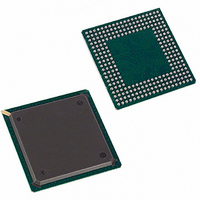
DS3112+W Maxim Integrated Products, DS3112+W Datasheet - Page 29

DS3112+W
Manufacturer Part Number
DS3112+W
Description
IC MUX T3/E3 3.3V 256-PBGA
Manufacturer
Maxim Integrated Products
Datasheet
1.DS3112.pdf
(133 pages)
Specifications of DS3112+W
Controller Type
Framer, Multiplexer
Interface
Parallel/Serial
Voltage - Supply
3.135 V ~ 3.465 V
Current - Supply
150mA
Operating Temperature
0°C ~ 70°C
Mounting Type
Surface Mount
Package / Case
256-PBGA
Lead Free Status / RoHS Status
Lead free / RoHS Compliant
- Current page: 29 of 133
- Download datasheet (3Mb)
2.9 JTAG Signal Description
Signal Name:
Signal Description:
Signal Type:
This signal is used to shift data into JTDI on the rising edge and out of JTDO on the falling edge. If not
used, this signal should be pulled high.
Signal Name:
Signal Description:
Signal Type:
Test instructions and data are clocked into this signal on the rising edge of JTCLK. If not used, this signal
should be pulled high. This signal has an internal pullup.
Signal Name:
Signal Description:
Signal Type:
Test instructions are clocked out of this signal on the falling edge of JTCLK. If not used, this signal
should be left open circuited.
Signal Name:
Signal Description:
Signal Type:
This signal is used to asynchronously reset the test access port controller. At power-up, JTRST must be
set low and then high. This action will set the device into the boundary scan bypass mode allowing
normal device operation. If boundary scan is not used, this signal should be held low. This signal has an
internal pullup.
Signal Name:
Signal Description:
Signal Type:
This signal is sampled on the rising edge of JTCLK and is used to place the test port into the various
defined IEEE 1149.1 states. If not used, this signal should be pulled high. This signal has an internal
pullup.
2.10 Supply, Test, Reset, and Mode Signal Description
Signal Name:
Signal Description:
Signal Type:
This active low asynchronous signal causes the device to be reset. When this signal is forced low, it
causes all of the internal registers to be forced to 00h and the high-speed T3/E3 ports as well as the low-
speed T1/E1 ports to source an unframed all ones data pattern. The device will be held in a reset state as
long as this signal is low. This signal should be activated after the hardware configuration signals (LIEN
and T3E3MS) and the clocks (FTCLK, LTCLK, HRCLK, and LITCLK) are stable and must be returned
high before the device can be configured for operation.
JTCLK
JTAG IEEE 1149.1 Test Serial Clock
Input
JTDI
JTAG IEEE 1149.1 Test Serial Data Input
Input (with internal 10kΩ pullup)
JTDO
JTAG IEEE 1149.1 Test Serial Data Output
Output
JTRST
JTAG IEEE 1149.1 Test Reset
Input (with internal 10kΩ pullup)
JTMS
JTAG IEEE 1149.1 Test Mode Select
Input (with internal 10kΩ pullup)
RST*
Global Hardware Reset
Input (with internal 10kΩ pullup)
29 of 133
DS3112
Related parts for DS3112+W
Image
Part Number
Description
Manufacturer
Datasheet
Request
R

Part Number:
Description:
IC MUX TEMPE T3/E3 256-BGA
Manufacturer:
Maxim Integrated Products
Datasheet:

Part Number:
Description:
IC MUX TEMPE T3/E3 256-BGA
Manufacturer:
Maxim Integrated Products
Datasheet:

Part Number:
Description:
IC FRAMER DS3/E3 SNGL 144CSBGA
Manufacturer:
Maxim Integrated Products
Datasheet:

Part Number:
Description:
IC 8CH DS3/3 FRAMER 349-BGA
Manufacturer:
Maxim Integrated Products
Datasheet:

Part Number:
Description:
IC 8CH DS3/3 FRAMER 349-BGA
Manufacturer:
Maxim Integrated Products
Datasheet:

Part Number:
Description:
IC 12CH DS3/3 FRAMER 349-BGA
Manufacturer:
Maxim Integrated Products
Datasheet:

Part Number:
Description:
IC 12CH DS3/3 FRAMER 349-BGA
Manufacturer:
Maxim Integrated Products
Datasheet:

Part Number:
Description:
MAX7528KCWPMaxim Integrated Products [CMOS Dual 8-Bit Buffered Multiplying DACs]
Manufacturer:
Maxim Integrated Products
Datasheet:

Part Number:
Description:
Single +5V, fully integrated, 1.25Gbps laser diode driver.
Manufacturer:
Maxim Integrated Products
Datasheet:

Part Number:
Description:
Single +5V, fully integrated, 155Mbps laser diode driver.
Manufacturer:
Maxim Integrated Products
Datasheet:

Part Number:
Description:
VRD11/VRD10, K8 Rev F 2/3/4-Phase PWM Controllers with Integrated Dual MOSFET Drivers
Manufacturer:
Maxim Integrated Products
Datasheet:

Part Number:
Description:
Highly Integrated Level 2 SMBus Battery Chargers
Manufacturer:
Maxim Integrated Products
Datasheet:

Part Number:
Description:
Current Monitor and Accumulator with Integrated Sense Resistor; ; Temperature Range: -40°C to +85°C
Manufacturer:
Maxim Integrated Products

Part Number:
Description:
TSSOP 14/A°/RS-485 Transceivers with Integrated 100O/120O Termination Resis
Manufacturer:
Maxim Integrated Products

Part Number:
Description:
TSSOP 14/A°/RS-485 Transceivers with Integrated 100O/120O Termination Resis
Manufacturer:
Maxim Integrated Products


