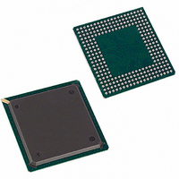
DS3112+W Maxim Integrated Products, DS3112+W Datasheet - Page 28

DS3112+W
Manufacturer Part Number
DS3112+W
Description
IC MUX T3/E3 3.3V 256-PBGA
Manufacturer
Maxim Integrated Products
Datasheet
1.DS3112.pdf
(133 pages)
Specifications of DS3112+W
Controller Type
Framer, Multiplexer
Interface
Parallel/Serial
Voltage - Supply
3.135 V ~ 3.465 V
Current - Supply
150mA
Operating Temperature
0°C ~ 70°C
Mounting Type
Surface Mount
Package / Case
256-PBGA
Lead Free Status / RoHS Status
Lead free / RoHS Compliant
- Current page: 28 of 133
- Download datasheet (3Mb)
2.7 High-Speed (T3 or E3) Receive Port Signal Description
Signal Name:
Signal Description:
Signal Type:
These input signals sample the serial data from the incoming T3 data streams or E3 data streams. Data
can be clocked into the device either on rising edges (normal clock mode) or falling edges (inverted clock
mode) of the associated HRCLK. This option is controlled via the HRCLKI control bit in Master Control
Register 2 (Section 4.2).
Signal Name:
Signal Description:
Signal Type:
This signal is used to clock data in from the incoming T3 or E3 data streams. The T3 or E3 serial data
streams at the HRPOS and HRNEG signals can be clocked into the device either on rising edges (normal
clock mode) or falling edges (inverted clock mode) of HRCLK. This option is controlled via the HRCLKI
control bit in Master Control Register 2 (Section 4.2).
Note: The HRCLK must be present for the host to be able to obtain status information (except the LOTC
and LORC status bits, see Section 4.3) from the device.
2.8 High-Speed (T3 or E3) Transmit Port Signal Description
Signal Name:
Signal Description:
Signal Type:
These output signals present the outgoing T3 data streams or E3 data streams. Data can be clocked out of
the device either on rising edges (normal clock mode) or falling edges (inverted clock mode) of HTCLK.
This option is controlled via the HTCLKI control bit in Master Control Register 2 (Section 4.2). Also,
these outputs can be forced high or low via the HTDATH and HTDATL control bits respectively in
Master Control Register 2 (Section 4.2).
Signal Name:
Signal Description:
Signal Type:
This output signal is used to clock T3 or E3 data out of the device. The T3 or E3 serial data streams at the
HTPOS and HTNEG signals can be clocked out of the device either on rising edges (normal clock mode)
or falling edges (inverted clock mode) of HTCLK. This option is controlled via the HTCLKI control bit
in Master Control Register 2 (Section 4.2).
HRPOS/HRNEG
High-Speed (T3 or E3) Receive Serial Data Inputs
Input
HRCLK
High-Speed (T3 or E3) Receive Serial Clock Input
Input
HTPOS/HTNEG
High-Speed (T3 or E3) Transmit Serial Data Outputs
Output
HTCLK
High-Speed (T3 or E3) Transmit Serial Clock Output
Output
28 of 133
DS3112
Related parts for DS3112+W
Image
Part Number
Description
Manufacturer
Datasheet
Request
R

Part Number:
Description:
IC MUX TEMPE T3/E3 256-BGA
Manufacturer:
Maxim Integrated Products
Datasheet:

Part Number:
Description:
IC MUX TEMPE T3/E3 256-BGA
Manufacturer:
Maxim Integrated Products
Datasheet:

Part Number:
Description:
IC FRAMER DS3/E3 SNGL 144CSBGA
Manufacturer:
Maxim Integrated Products
Datasheet:

Part Number:
Description:
IC 8CH DS3/3 FRAMER 349-BGA
Manufacturer:
Maxim Integrated Products
Datasheet:

Part Number:
Description:
IC 8CH DS3/3 FRAMER 349-BGA
Manufacturer:
Maxim Integrated Products
Datasheet:

Part Number:
Description:
IC 12CH DS3/3 FRAMER 349-BGA
Manufacturer:
Maxim Integrated Products
Datasheet:

Part Number:
Description:
IC 12CH DS3/3 FRAMER 349-BGA
Manufacturer:
Maxim Integrated Products
Datasheet:

Part Number:
Description:
MAX7528KCWPMaxim Integrated Products [CMOS Dual 8-Bit Buffered Multiplying DACs]
Manufacturer:
Maxim Integrated Products
Datasheet:

Part Number:
Description:
Single +5V, fully integrated, 1.25Gbps laser diode driver.
Manufacturer:
Maxim Integrated Products
Datasheet:

Part Number:
Description:
Single +5V, fully integrated, 155Mbps laser diode driver.
Manufacturer:
Maxim Integrated Products
Datasheet:

Part Number:
Description:
VRD11/VRD10, K8 Rev F 2/3/4-Phase PWM Controllers with Integrated Dual MOSFET Drivers
Manufacturer:
Maxim Integrated Products
Datasheet:

Part Number:
Description:
Highly Integrated Level 2 SMBus Battery Chargers
Manufacturer:
Maxim Integrated Products
Datasheet:

Part Number:
Description:
Current Monitor and Accumulator with Integrated Sense Resistor; ; Temperature Range: -40°C to +85°C
Manufacturer:
Maxim Integrated Products

Part Number:
Description:
TSSOP 14/A°/RS-485 Transceivers with Integrated 100O/120O Termination Resis
Manufacturer:
Maxim Integrated Products

Part Number:
Description:
TSSOP 14/A°/RS-485 Transceivers with Integrated 100O/120O Termination Resis
Manufacturer:
Maxim Integrated Products


