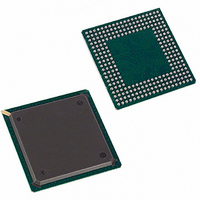
DS3112+W Maxim Integrated Products, DS3112+W Datasheet - Page 33

DS3112+W
Manufacturer Part Number
DS3112+W
Description
IC MUX T3/E3 3.3V 256-PBGA
Manufacturer
Maxim Integrated Products
Datasheet
1.DS3112.pdf
(133 pages)
Specifications of DS3112+W
Controller Type
Framer, Multiplexer
Interface
Parallel/Serial
Voltage - Supply
3.135 V ~ 3.465 V
Current - Supply
150mA
Operating Temperature
0°C ~ 70°C
Mounting Type
Surface Mount
Package / Case
256-PBGA
Lead Free Status / RoHS Status
Lead free / RoHS Compliant
- Current page: 33 of 133
- Download datasheet (3Mb)
4 MASTER DEVICE CONFIGURATION AND STATUS/INTERRUPT
4.1 Master Reset and ID Register Description
The master reset and ID (MRID) register can be used to globally reset the device. When the RST bit is set
to one, all of the internal registers will be placed into their default state, which is 0000h. A reset can also
be invoked by the RST hardware signal.
The upper byte of the MRID register is read-only and it can be read by the host to determine the chip
revision. Contact the factory for specifics on the meaning of the value read from the ID0 to ID7 bits.
Register Name:
Register Description:
Register Address:
Bit #
Name
Default
Bit #
Name
Default
Note: Bits that are underlined are read-only; all other bits are read-write.
Bit 0: Master Software Reset (RST). When this bit is set to a one by the host, it will force all of the internal
registers to their default state, which is 0000h and forces the T3/E3 and T1/E1 outputs to send an all ones pattern.
This bit must be set high for a minimum of 100ns. This software bit is logically ORed with the hardware signal
RST.
Bit 1: Low-Speed (T1/E1) Receive FIFO Reset (RFIFOR). A zero to one transition on this bit will cause the
receive T1/E1 demux FIFOs to be reset, which will cause them to be flushed. See the DS3112 Block Diagrams in
Figure 1-1
set again for a subsequent reset to occur.
Bit 2: T2/E2/G.747 Force Receive Framer Resynchronization (T2E2RSY). A zero to one transition on this bit
will cause all seven of the T2 receive framers or all four of the E2 receive framers or all seven of the G.747 framers
to resynchronize. This bit must be cleared and set again for a subsequent resynchronization to occur.
Bit 3: T3/E3 Force Receive Framer Resynchronization (T3E3RSY). A zero to one transition on this bit will
cause the T3 receive framer or the E3 receive framer to resynchronize. This bit must be cleared and set again for a
subsequent resynchronization to occur.
Bits 8 to 15: Chip Revision ID Bit 0 to 7 (ID0 to ID7). Read-only. Contact the factory for details on the meaning
of the ID bits.
0 = normal operation
1 = force all internal registers to their default value of 0000h
and
Figure 1-2
ID7
—
—
15
X
7
for details on the placement of the FIFOs within the chip. This bit must be cleared and
ID6
—
—
14
X
6
MRID
Master Reset and ID Register
00h
ID5
—
—
13
X
5
33 of 133
—
—
ID4
4
12
X
T3E3RSY
ID3
3
0
11
X
T2E2RSY
ID2
10
X
2
0
RFIFOR
ID1
X
9
1
0
ID0
RST
X
8
DS3112
0
0
Related parts for DS3112+W
Image
Part Number
Description
Manufacturer
Datasheet
Request
R

Part Number:
Description:
IC MUX TEMPE T3/E3 256-BGA
Manufacturer:
Maxim Integrated Products
Datasheet:

Part Number:
Description:
IC MUX TEMPE T3/E3 256-BGA
Manufacturer:
Maxim Integrated Products
Datasheet:

Part Number:
Description:
IC FRAMER DS3/E3 SNGL 144CSBGA
Manufacturer:
Maxim Integrated Products
Datasheet:

Part Number:
Description:
IC 8CH DS3/3 FRAMER 349-BGA
Manufacturer:
Maxim Integrated Products
Datasheet:

Part Number:
Description:
IC 8CH DS3/3 FRAMER 349-BGA
Manufacturer:
Maxim Integrated Products
Datasheet:

Part Number:
Description:
IC 12CH DS3/3 FRAMER 349-BGA
Manufacturer:
Maxim Integrated Products
Datasheet:

Part Number:
Description:
IC 12CH DS3/3 FRAMER 349-BGA
Manufacturer:
Maxim Integrated Products
Datasheet:

Part Number:
Description:
MAX7528KCWPMaxim Integrated Products [CMOS Dual 8-Bit Buffered Multiplying DACs]
Manufacturer:
Maxim Integrated Products
Datasheet:

Part Number:
Description:
Single +5V, fully integrated, 1.25Gbps laser diode driver.
Manufacturer:
Maxim Integrated Products
Datasheet:

Part Number:
Description:
Single +5V, fully integrated, 155Mbps laser diode driver.
Manufacturer:
Maxim Integrated Products
Datasheet:

Part Number:
Description:
VRD11/VRD10, K8 Rev F 2/3/4-Phase PWM Controllers with Integrated Dual MOSFET Drivers
Manufacturer:
Maxim Integrated Products
Datasheet:

Part Number:
Description:
Highly Integrated Level 2 SMBus Battery Chargers
Manufacturer:
Maxim Integrated Products
Datasheet:

Part Number:
Description:
Current Monitor and Accumulator with Integrated Sense Resistor; ; Temperature Range: -40°C to +85°C
Manufacturer:
Maxim Integrated Products

Part Number:
Description:
TSSOP 14/A°/RS-485 Transceivers with Integrated 100O/120O Termination Resis
Manufacturer:
Maxim Integrated Products

Part Number:
Description:
TSSOP 14/A°/RS-485 Transceivers with Integrated 100O/120O Termination Resis
Manufacturer:
Maxim Integrated Products


