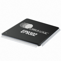
EP9302-CQZ Cirrus Logic Inc, EP9302-CQZ Datasheet - Page 505

EP9302-CQZ
Manufacturer Part Number
EP9302-CQZ
Description
IC ARM9 SOC PROCESSOR 208LQFP
Manufacturer
Cirrus Logic Inc
Series
EP9r
Datasheets
1.EP9307-CRZ.pdf
(824 pages)
2.EP9302-IQZ.pdf
(42 pages)
3.EP9302-IQZ.pdf
(4 pages)
4.EP9302-IQZ.pdf
(40 pages)
Specifications of EP9302-CQZ
Program Memory Type
ROMless
Package / Case
208-LQFP
Core Processor
ARM9
Core Size
16/32-Bit
Speed
200MHz
Connectivity
EBI/EMI, Ethernet, I²C, IrDA, SPI, UART/USART, USB
Peripherals
AC'97, DMA, I²:S, LED, MaverickKey, POR, PWM, WDT
Number Of I /o
19
Ram Size
32K x 8
Voltage - Supply (vcc/vdd)
1.65 V ~ 3.6 V
Data Converters
A/D 5x12b
Oscillator Type
External
Operating Temperature
0°C ~ 70°C
Processor Series
EP93xx
Core
ARM920T
Data Bus Width
32 bit
Data Ram Size
16 bit
Interface Type
USB, USART, SPI
Maximum Clock Frequency
200 MHz
Number Of Programmable I/os
37
Mounting Style
SMD/SMT
3rd Party Development Tools
MDK-ARM, RL-ARM, ULINK2
Development Tools By Supplier
EDB9302A-Z
Controller Family/series
(ARM9)
No. Of I/o's
19
Ram Memory Size
16MB
Cpu Speed
200MHz
No. Of Timers
4
Embedded Interface Type
AC97, I2S, SPI, UART, USB
Rohs Compliant
Yes
Lead Free Status / RoHS Status
Lead free / RoHS Compliant
For Use With
598-1132 - KIT DEVELOPMENT EP9302 ARM9
Eeprom Size
-
Program Memory Size
-
Lead Free Status / Rohs Status
Lead free / RoHS Compliant
Other names
598-1137
Available stocks
Company
Part Number
Manufacturer
Quantity
Price
Company:
Part Number:
EP9302-CQZ
Manufacturer:
Cirrus
Quantity:
3 295
Company:
Part Number:
EP9302-CQZ
Manufacturer:
ALTERA
Quantity:
672
Part Number:
EP9302-CQZ
Manufacturer:
CYPRESS/赛普拉斯
Quantity:
20 000
- EP9307-CRZ PDF datasheet
- EP9302-IQZ PDF datasheet #2
- EP9302-IQZ PDF datasheet #3
- EP9302-IQZ PDF datasheet #4
- Current page: 505 of 824
- Download datasheet (13Mb)
DS785UM1
13.8.1 Chip Select SDCSN[3:0] Decoding
13.8 External Synchronous Memory System
to the SyncFLASH register and the associated value on the data pins specifies which
SyncFLASH register is written. Actually, the value on the data pins specifies a command to
the SyncFLASH device such as Write Configuration Register, Lock Block, Block Erase; and
the associated value on the address pins specifies either a value that is written to a register
or a address location inside the SyncFLASH device.
Synchronous FLASH devices:
The synchronous memory system is decoded from the ARM Core’s physical memory map
into four independent address domains, each having an address range of 256 Mbytes (64
Mwords). All of the memory devices that are attached to a given domain must be of the same
type, but the other domains may use different memory device types and associated timing
characteristics.
Since all memory devices, synchronous or static, share a common external memory bus, the
total number of devices is limited by the maximum allowable bus capacitance.
Each of the four address domains within synchronous memory space have an associated
chip select signal that is output on one of the SDCSn[3:0] pins as shown in
signals are decoded from address bits A31:A28.
The latched value of ASDO determines how SDCSn3 is mapped into synchronous memory
space. If the latched value of ASDO=1 then SDCSn3 is mapped to 0x0000_0000 otherwise it
is mapped to 0xF000_0000.
• Use the same combination of the CS, RAS, CAS, and WE signals which would normally
• Cannot be written in bursts, but only one word at a time. Hence the requirement to write
• Require 100 μs of initialization time after a low-to-high transition occurs on its write
• Can be set up by either programming the Synchronous FLASH Configuration register
place an SDRAM device into Auto-Refresh mode
WBM = ‘1’ to the appropriate SDRAMDevCfg register. When WBM = ‘1’, no Auto
Refresh cycle will occur in the associated synchronous memory domain because the
synchronous memory controller will assume that a Synchronous FLASH device is
attached.
protect input pin
before releasing the processor from reset or by using the contents of it’s
NonVolatileMODE register (which must have been previously programmed).
Boot Option
(ASDO)
1
A31
0
Table 13-9. Chip Select Decoding
Copyright 2007 Cirrus Logic
A30
0
A29
0
SDRAM, SyncROM, and SyncFLASH Controller
A28
0
Chip select
nSDCS3
EP93xx User’s Guide
Table
13-9. These
13-9
13
Related parts for EP9302-CQZ
Image
Part Number
Description
Manufacturer
Datasheet
Request
R

Part Number:
Description:
IC ARM9 SOC PROCESSOR 208LQFP
Manufacturer:
Cirrus Logic Inc
Datasheet:

Part Number:
Description:
High Performance, Entry Level ARM9 SoC
Manufacturer:
Cirrus Logic Inc

Part Number:
Description:
MCU, MPU & DSP Development Tools Eval Bd Hgh-Prfrmnc ARM9 SOC Processor
Manufacturer:
Cirrus Logic Inc
Datasheet:

Part Number:
Description:
Development Kit
Manufacturer:
Cirrus Logic Inc
Datasheet:

Part Number:
Description:
Development Kit
Manufacturer:
Cirrus Logic Inc
Datasheet:

Part Number:
Description:
High-efficiency PFC + Fluorescent Lamp Driver Reference Design
Manufacturer:
Cirrus Logic Inc
Datasheet:

Part Number:
Description:
Development Kit
Manufacturer:
Cirrus Logic Inc
Datasheet:

Part Number:
Description:
Development Kit
Manufacturer:
Cirrus Logic Inc
Datasheet:

Part Number:
Description:
Development Kit
Manufacturer:
Cirrus Logic Inc
Datasheet:

Part Number:
Description:
Development Kit
Manufacturer:
Cirrus Logic Inc
Datasheet:

Part Number:
Description:
Development Kit
Manufacturer:
Cirrus Logic Inc
Datasheet:

Part Number:
Description:
Ref Bd For Speakerbar MSA & DSP Products
Manufacturer:
Cirrus Logic Inc


