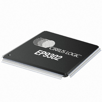
EP9302-CQZ Cirrus Logic Inc, EP9302-CQZ Datasheet - Page 489

EP9302-CQZ
Manufacturer Part Number
EP9302-CQZ
Description
IC ARM9 SOC PROCESSOR 208LQFP
Manufacturer
Cirrus Logic Inc
Series
EP9r
Datasheets
1.EP9307-CRZ.pdf
(824 pages)
2.EP9302-IQZ.pdf
(42 pages)
3.EP9302-IQZ.pdf
(4 pages)
4.EP9302-IQZ.pdf
(40 pages)
Specifications of EP9302-CQZ
Program Memory Type
ROMless
Package / Case
208-LQFP
Core Processor
ARM9
Core Size
16/32-Bit
Speed
200MHz
Connectivity
EBI/EMI, Ethernet, I²C, IrDA, SPI, UART/USART, USB
Peripherals
AC'97, DMA, I²:S, LED, MaverickKey, POR, PWM, WDT
Number Of I /o
19
Ram Size
32K x 8
Voltage - Supply (vcc/vdd)
1.65 V ~ 3.6 V
Data Converters
A/D 5x12b
Oscillator Type
External
Operating Temperature
0°C ~ 70°C
Processor Series
EP93xx
Core
ARM920T
Data Bus Width
32 bit
Data Ram Size
16 bit
Interface Type
USB, USART, SPI
Maximum Clock Frequency
200 MHz
Number Of Programmable I/os
37
Mounting Style
SMD/SMT
3rd Party Development Tools
MDK-ARM, RL-ARM, ULINK2
Development Tools By Supplier
EDB9302A-Z
Controller Family/series
(ARM9)
No. Of I/o's
19
Ram Memory Size
16MB
Cpu Speed
200MHz
No. Of Timers
4
Embedded Interface Type
AC97, I2S, SPI, UART, USB
Rohs Compliant
Yes
Lead Free Status / RoHS Status
Lead free / RoHS Compliant
For Use With
598-1132 - KIT DEVELOPMENT EP9302 ARM9
Eeprom Size
-
Program Memory Size
-
Lead Free Status / Rohs Status
Lead free / RoHS Compliant
Other names
598-1137
Available stocks
Company
Part Number
Manufacturer
Quantity
Price
Company:
Part Number:
EP9302-CQZ
Manufacturer:
Cirrus
Quantity:
3 295
Company:
Part Number:
EP9302-CQZ
Manufacturer:
ALTERA
Quantity:
672
Part Number:
EP9302-CQZ
Manufacturer:
CYPRESS/赛普拉斯
Quantity:
20 000
- EP9307-CRZ PDF datasheet
- EP9302-IQZ PDF datasheet #2
- EP9302-IQZ PDF datasheet #3
- EP9302-IQZ PDF datasheet #4
- Current page: 489 of 824
- Download datasheet (13Mb)
DS785UM1
Bit Descriptions:
RSVD:
IDCY:
WST1:
RBLE:
WST2:
Copyright 2007 Cirrus Logic
• A single Read or Write access, or
• The first Read or Write access of a burst-of-four
Reserved - Unknown During Read
Idle Cycle - Read/Write
The value written to this field specifies the memory data
bus turnaround time between a Read access and a Write
access. The turnaround time is specified by (IDCY + 1)
HCLKs. For example, if IDCY = 0xA, the turnaround time
is 10 + 1 = 11 cycles of HCLK.
Wait States1 - Read/Write
The value written to this field specifies the ‘number of
HCLK cycles, minus 1’ that are inserted as wait cycles into
the timing for:
The number of wait cycles is specified by (WST1 + 1)
HCLKs. For example, if WST1 = 0x3, 3 + 1 = 4 cycles of
HCLK are inserted into the access timing.
On reset, this field defaults to 0x1F (slowest access) to
enable booting from ROM or FLASH memory device
types.
Read Byte Lane Enable - Read/Write
The value written to this bit specifies the output values on
the DQMn[3:0] pins during a Read access:
0 - DQMn[3:0] pins are all driven HIGH during memory
Reads (default at reset for bank 1-3,6,7)
1 - DQMn[3:0] pins are all driven LOW during memory
Reads (default at reset for bank 0)
For memory Writes, this bit must written to ‘1’.
Wait States2 - Read/Write
The value in this field specifies the ‘number of HCLK
cycles, minus 1’ that are inserted as wait cycles into the
timing for each of the 2nd, 3rd, and 4th accesses of Read
or Write burst-of-four accesses.
accesses.
Static Memory Controller
EP93xx User’s Guide
12-11
12
Related parts for EP9302-CQZ
Image
Part Number
Description
Manufacturer
Datasheet
Request
R

Part Number:
Description:
IC ARM9 SOC PROCESSOR 208LQFP
Manufacturer:
Cirrus Logic Inc
Datasheet:

Part Number:
Description:
High Performance, Entry Level ARM9 SoC
Manufacturer:
Cirrus Logic Inc

Part Number:
Description:
MCU, MPU & DSP Development Tools Eval Bd Hgh-Prfrmnc ARM9 SOC Processor
Manufacturer:
Cirrus Logic Inc
Datasheet:

Part Number:
Description:
Development Kit
Manufacturer:
Cirrus Logic Inc
Datasheet:

Part Number:
Description:
Development Kit
Manufacturer:
Cirrus Logic Inc
Datasheet:

Part Number:
Description:
High-efficiency PFC + Fluorescent Lamp Driver Reference Design
Manufacturer:
Cirrus Logic Inc
Datasheet:

Part Number:
Description:
Development Kit
Manufacturer:
Cirrus Logic Inc
Datasheet:

Part Number:
Description:
Development Kit
Manufacturer:
Cirrus Logic Inc
Datasheet:

Part Number:
Description:
Development Kit
Manufacturer:
Cirrus Logic Inc
Datasheet:

Part Number:
Description:
Development Kit
Manufacturer:
Cirrus Logic Inc
Datasheet:

Part Number:
Description:
Development Kit
Manufacturer:
Cirrus Logic Inc
Datasheet:

Part Number:
Description:
Ref Bd For Speakerbar MSA & DSP Products
Manufacturer:
Cirrus Logic Inc


