D6417760BP200ADV Renesas Electronics America, D6417760BP200ADV Datasheet - Page 743
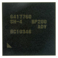
D6417760BP200ADV
Manufacturer Part Number
D6417760BP200ADV
Description
IC SUPER H MPU ROMLESS 256BGA
Manufacturer
Renesas Electronics America
Series
SuperH® SH7750r
Datasheet
1.D6417760BP200ADV.pdf
(1418 pages)
Specifications of D6417760BP200ADV
Core Processor
SH-4
Core Size
32-Bit
Speed
200MHz
Connectivity
Audio Codec, CAN, EBI/EMI, FIFO, I²C, MFI, MMC, SCI, Serial Sound, SIM, SPI, USB
Peripherals
DMA, LCD, POR, WDT
Number Of I /o
69
Program Memory Type
ROMless
Ram Size
48K x 8
Voltage - Supply (vcc/vdd)
1.4 V ~ 1.6 V
Data Converters
A/D 4x10b
Oscillator Type
Internal
Operating Temperature
-40°C ~ 85°C
Package / Case
256-BGA
Lead Free Status / RoHS Status
Lead free / RoHS Compliant
Eeprom Size
-
Program Memory Size
-
Available stocks
Company
Part Number
Manufacturer
Quantity
Price
Company:

Part Number:
D6417760BP200ADV
Manufacturer:
Renesas Electronics America
Quantity:
10 000


18.5.4
If the TEIE bit is always set to 1 during continuous transmission, unnecessary transmit end
interrupts (SIMTEI) occur because the TEND bit is set to 1 every time transmission is completed.
To avoid unnecessary SIMTEI requests, the TEIE bit in SISCR should be set to 1 only after the
last transmit data is written to SITDR and SITSR starts transmission.
Figure 18.10 shows the signal waveforms when TEIE is set to 1.
18.5.5
When switching between the smart card interface mode and standby mode, in order to maintain
the clock duty, the following switching procedure should be used. Figure 18.11 shows standby
mode switching procedure. (1) to (7) in figure 18.11 correspond to items 1 to 7 described below.
• When changing from smart card interface mode to standby mode:
SIMTEI
request
TEND
TDRE
TEIE
1. Write 0 to the TE and RE bits in SISCR, to stop transmission and reception operations. At
2. Write 0 to the CKE0 bit in SISCR to stop the clock.
3. Wait for one clock cycle of the serial clock. During this interval, the duty is maintained,
4. Make the transition to standby mode.
the same time, set the CKE1 bit to the value for the output-fixed state in standby mode.
and the clock output is fixed at the specified level.
(DE)
Transmit End Interrupt
Standby Mode Switching
Ds
D0 D1 D2 D3 D4 D5 D6 D7 DP
Transfer frame
Unnecessary TEND set timing
Figure 18.10 TEIE Set Timing
(DE)
Ds
D0 D1 D2 D3 D4 D5 D6 D7 DP
Transfer frame
Rev. 2.00 Feb. 12, 2010 Page 659 of 1330
(DE)
Ds
D0 D1 D2 D3 D4 D5 D6 D7 DP
TEIE set timing
Last frame
REJ09B0554-0200
Related parts for D6417760BP200ADV
Image
Part Number
Description
Manufacturer
Datasheet
Request
R

Part Number:
Description:
KIT STARTER FOR M16C/29
Manufacturer:
Renesas Electronics America
Datasheet:

Part Number:
Description:
KIT STARTER FOR R8C/2D
Manufacturer:
Renesas Electronics America
Datasheet:

Part Number:
Description:
R0K33062P STARTER KIT
Manufacturer:
Renesas Electronics America
Datasheet:

Part Number:
Description:
KIT STARTER FOR R8C/23 E8A
Manufacturer:
Renesas Electronics America
Datasheet:

Part Number:
Description:
KIT STARTER FOR R8C/25
Manufacturer:
Renesas Electronics America
Datasheet:

Part Number:
Description:
KIT STARTER H8S2456 SHARPE DSPLY
Manufacturer:
Renesas Electronics America
Datasheet:

Part Number:
Description:
KIT STARTER FOR R8C38C
Manufacturer:
Renesas Electronics America
Datasheet:

Part Number:
Description:
KIT STARTER FOR R8C35C
Manufacturer:
Renesas Electronics America
Datasheet:

Part Number:
Description:
KIT STARTER FOR R8CL3AC+LCD APPS
Manufacturer:
Renesas Electronics America
Datasheet:
Part Number:
Description:
KIT STARTER FOR RX610
Manufacturer:
Renesas Electronics America
Datasheet:

Part Number:
Description:
KIT STARTER FOR R32C/118
Manufacturer:
Renesas Electronics America
Datasheet:

Part Number:
Description:
KIT DEV RSK-R8C/26-29
Manufacturer:
Renesas Electronics America
Datasheet:

Part Number:
Description:
KIT STARTER FOR SH7124
Manufacturer:
Renesas Electronics America
Datasheet:

Part Number:
Description:
KIT STARTER FOR H8SX/1622
Manufacturer:
Renesas Electronics America
Datasheet:

Part Number:
Description:
KIT DEV FOR SH7203
Manufacturer:
Renesas Electronics America
Datasheet: