D6417760BP200ADV Renesas Electronics America, D6417760BP200ADV Datasheet - Page 403
D6417760BP200ADV
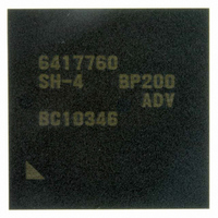
Manufacturer Part Number
D6417760BP200ADV
Description
IC SUPER H MPU ROMLESS 256BGA
Manufacturer
Renesas Electronics America
Series
SuperH® SH7750r
Datasheet
1.D6417760BP200ADV.pdf
(1418 pages)
Specifications of D6417760BP200ADV
Core Processor
SH-4
Core Size
32-Bit
Speed
200MHz
Connectivity
Audio Codec, CAN, EBI/EMI, FIFO, I²C, MFI, MMC, SCI, Serial Sound, SIM, SPI, USB
Peripherals
DMA, LCD, POR, WDT
Number Of I /o
69
Program Memory Type
ROMless
Ram Size
48K x 8
Voltage - Supply (vcc/vdd)
1.4 V ~ 1.6 V
Data Converters
A/D 4x10b
Oscillator Type
Internal
Operating Temperature
-40°C ~ 85°C
Package / Case
256-BGA
Lead Free Status / RoHS Status
Lead free / RoHS Compliant
Eeprom Size
-
Program Memory Size
-
Available stocks
Company
Part Number
Manufacturer
Quantity
Price
Company:

Part Number:
D6417760BP200ADV
Manufacturer:
Renesas Electronics America
Quantity:
10 000


Section 10 Bus State Controller (BSC)
A 32-byte burst transfer is performed in a cache fill/copy-back cycle. For write operations in the
write-through area and read/write operations in the non-cacheable area, 16-byte data is also read in
a single read because the synchronous DRAM is accessed by burst read/write operations with a
burst length of 4. Transfer of 16-byte data is also performed in a single write, but DQMn is not
asserted when unnecessary data is transferred.
This LSI also supports read and burst read and burst write modes with a burst length of 8 as a
synchronous DRAM operating mode. The data bus width is 32 bits, and the SZ bits in MCR must
be set to 11. A 32-byte burst transfer is performed in a cache fill/copy-back cycle. For write
operations in the write-through area and read/write operations in the non-cacheable area, 32-byte
data is also read in a single read because the synchronous DRAM is accessed by burst read/write
operations with a burst length of 8. Transfer of 32-byte data is also performed in a single write, but
DQMn is not asserted when unnecessary data is transferred. For details of setting a burst length of
8, refer to (11) Changing the Burst Length, in section 10.6.4. For details of burst length, refer to
section 10.5.11, Synchronous DRAM Mode Register (SDMR), and (10) Power-on Sequence, in
section 10.6.4.
The control signals for connecting synchronous DRAM are RAS, CASS, RD/WR, CS2 or CS3,
DQM0 to DQM3, and CKE. All signals other than CS2 and CS3 are common to all areas, and
signals other than CKE are valid and latched only when CS2 or CS3 is asserted. Synchronous
DRAM can therefore be connected in parallel to multiple areas. CKE is negated (to low level)
when the frequency is changed, when the clock is unstable during stopping of the clock or
restarting of the clock supply, or when self-refreshing is performed. Otherwise, CKE is always
asserted (to high level).
RAS, CASS, RD/WR, and specific address signals specify commands for synchronous DRAM.
The commands are NOP, auto-refresh (REF), self-refresh (SELF), precharge all banks (PALL),
precharge specified bank (PRE), row address strobe bank active (ACTV), read (READ), read with
precharge (READA), write (WRIT), write with precharge (WRITA), and mode register setting
(MRS).
Bytes are specified by DQM0 to DQM3. A read/write is performed for the byte where the
corresponding DQM signal is low. When the bus width is 32 bits in big-endian mode, DQM3
specifies an access to address 4n and DQM0 specifies an access to address 4n + 3. In little-endian
mode, DQM3 specifies an access to address 4n + 3 and DQM0 specifies an access to address 4n.
Rev. 2.00 Feb. 12, 2010 Page 319 of 1330
REJ09B0554-0200
Related parts for D6417760BP200ADV
Image
Part Number
Description
Manufacturer
Datasheet
Request
R

Part Number:
Description:
KIT STARTER FOR M16C/29
Manufacturer:
Renesas Electronics America
Datasheet:

Part Number:
Description:
KIT STARTER FOR R8C/2D
Manufacturer:
Renesas Electronics America
Datasheet:

Part Number:
Description:
R0K33062P STARTER KIT
Manufacturer:
Renesas Electronics America
Datasheet:

Part Number:
Description:
KIT STARTER FOR R8C/23 E8A
Manufacturer:
Renesas Electronics America
Datasheet:

Part Number:
Description:
KIT STARTER FOR R8C/25
Manufacturer:
Renesas Electronics America
Datasheet:

Part Number:
Description:
KIT STARTER H8S2456 SHARPE DSPLY
Manufacturer:
Renesas Electronics America
Datasheet:

Part Number:
Description:
KIT STARTER FOR R8C38C
Manufacturer:
Renesas Electronics America
Datasheet:

Part Number:
Description:
KIT STARTER FOR R8C35C
Manufacturer:
Renesas Electronics America
Datasheet:

Part Number:
Description:
KIT STARTER FOR R8CL3AC+LCD APPS
Manufacturer:
Renesas Electronics America
Datasheet:
Part Number:
Description:
KIT STARTER FOR RX610
Manufacturer:
Renesas Electronics America
Datasheet:

Part Number:
Description:
KIT STARTER FOR R32C/118
Manufacturer:
Renesas Electronics America
Datasheet:

Part Number:
Description:
KIT DEV RSK-R8C/26-29
Manufacturer:
Renesas Electronics America
Datasheet:

Part Number:
Description:
KIT STARTER FOR SH7124
Manufacturer:
Renesas Electronics America
Datasheet:

Part Number:
Description:
KIT STARTER FOR H8SX/1622
Manufacturer:
Renesas Electronics America
Datasheet:

Part Number:
Description:
KIT DEV FOR SH7203
Manufacturer:
Renesas Electronics America
Datasheet: