D6417760BP200ADV Renesas Electronics America, D6417760BP200ADV Datasheet - Page 419
D6417760BP200ADV
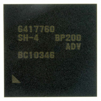
Manufacturer Part Number
D6417760BP200ADV
Description
IC SUPER H MPU ROMLESS 256BGA
Manufacturer
Renesas Electronics America
Series
SuperH® SH7750r
Datasheet
1.D6417760BP200ADV.pdf
(1418 pages)
Specifications of D6417760BP200ADV
Core Processor
SH-4
Core Size
32-Bit
Speed
200MHz
Connectivity
Audio Codec, CAN, EBI/EMI, FIFO, I²C, MFI, MMC, SCI, Serial Sound, SIM, SPI, USB
Peripherals
DMA, LCD, POR, WDT
Number Of I /o
69
Program Memory Type
ROMless
Ram Size
48K x 8
Voltage - Supply (vcc/vdd)
1.4 V ~ 1.6 V
Data Converters
A/D 4x10b
Oscillator Type
Internal
Operating Temperature
-40°C ~ 85°C
Package / Case
256-BGA
Lead Free Status / RoHS Status
Lead free / RoHS Compliant
Eeprom Size
-
Program Memory Size
-
Available stocks
Company
Part Number
Manufacturer
Quantity
Price
Company:

Part Number:
D6417760BP200ADV
Manufacturer:
Renesas Electronics America
Quantity:
10 000


addresses in the same bank, the PRE command cannot be issued until one cycle before the last
data latch cycle. If a write access follows a read access, a PRE or ACTV command can be issued
depending on the bank and row address, but since the write data is output at the same time as the
WRIT command, the PRE, ACTV, and WRIT commands are issued so that one or two dummy
cycles occur automatically on the data bus. Similarly, when a read access follows a write access,
or a write access follows a write access, the PRE, ACTV, or READ command is issued during the
data write cycle for the preceding access. However, a PRE command cannot be issued for different
row addresses in the same bank, and so the PRE command is issued following the number of Trwl
cycles specified by the TRWL bit in MCR after the end of the last data write cycle.
Figure 10.26 shows a burst read cycle for different banks and row addresses from the preceding
burst read cycle.
Pipelined access is enabled only for consecutive access to area 3, and is aborted when there is an
access to another area. Pipelined access is also aborted in the event of a refresh cycle, or bus
release due to bus arbitration. The cases where pipelined access is available are shown in table
10.17. In this table, DMAC dual indicates transfer by DMAC dual address mode, and DMAC
single indicates transfer by DMAC single address mode.
Address
CKIO
Bank
Precharge-sel
CSn
RD/WR
RAS
CASS
DQMn
BS
CKE
D31-D0
(read)
Figure 10.26 Burst Read Cycle for Different Bank and Row Address From Preceding Burst
Tc1_A
c1_A
H/L
a1
c5_A
Read Cycle
H/L
a2
a3
a4
Rev. 2.00 Feb. 12, 2010 Page 335 of 1330
a5
Tc1_B
c1_B
H/L
a6
a7
a8
REJ09B0554-0200
b1
c5_B
H/L
b2
Related parts for D6417760BP200ADV
Image
Part Number
Description
Manufacturer
Datasheet
Request
R

Part Number:
Description:
KIT STARTER FOR M16C/29
Manufacturer:
Renesas Electronics America
Datasheet:

Part Number:
Description:
KIT STARTER FOR R8C/2D
Manufacturer:
Renesas Electronics America
Datasheet:

Part Number:
Description:
R0K33062P STARTER KIT
Manufacturer:
Renesas Electronics America
Datasheet:

Part Number:
Description:
KIT STARTER FOR R8C/23 E8A
Manufacturer:
Renesas Electronics America
Datasheet:

Part Number:
Description:
KIT STARTER FOR R8C/25
Manufacturer:
Renesas Electronics America
Datasheet:

Part Number:
Description:
KIT STARTER H8S2456 SHARPE DSPLY
Manufacturer:
Renesas Electronics America
Datasheet:

Part Number:
Description:
KIT STARTER FOR R8C38C
Manufacturer:
Renesas Electronics America
Datasheet:

Part Number:
Description:
KIT STARTER FOR R8C35C
Manufacturer:
Renesas Electronics America
Datasheet:

Part Number:
Description:
KIT STARTER FOR R8CL3AC+LCD APPS
Manufacturer:
Renesas Electronics America
Datasheet:
Part Number:
Description:
KIT STARTER FOR RX610
Manufacturer:
Renesas Electronics America
Datasheet:

Part Number:
Description:
KIT STARTER FOR R32C/118
Manufacturer:
Renesas Electronics America
Datasheet:

Part Number:
Description:
KIT DEV RSK-R8C/26-29
Manufacturer:
Renesas Electronics America
Datasheet:

Part Number:
Description:
KIT STARTER FOR SH7124
Manufacturer:
Renesas Electronics America
Datasheet:

Part Number:
Description:
KIT STARTER FOR H8SX/1622
Manufacturer:
Renesas Electronics America
Datasheet:

Part Number:
Description:
KIT DEV FOR SH7203
Manufacturer:
Renesas Electronics America
Datasheet: