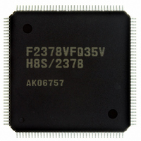
DF61657CN35FTV Renesas Electronics America, DF61657CN35FTV Datasheet - Page 738

DF61657CN35FTV
Manufacturer Part Number
DF61657CN35FTV
Description
IC H8SX/1657 MCU FLASH 120TQFP
Manufacturer
Renesas Electronics America
Series
H8® H8SX/1600r
Datasheet
1.DF61656N35FTV.pdf
(894 pages)
Specifications of DF61657CN35FTV
Core Processor
H8SX
Core Size
32-Bit
Speed
35MHz
Connectivity
SCI, SmartCard
Peripherals
DMA, PWM, WDT
Number Of I /o
82
Program Memory Size
768KB (768K x 8)
Program Memory Type
FLASH
Ram Size
24K x 8
Voltage - Supply (vcc/vdd)
3 V ~ 3.6 V
Data Converters
A/D 8x10b; D/A 2x8b
Oscillator Type
Internal
Operating Temperature
-20°C ~ 75°C
Package / Case
120-TQFP, 120-VQFP
For Use With
3DK1657 - DEV EVAL KIT FOR H8SX/1657
Lead Free Status / RoHS Status
Lead free / RoHS Compliant
Eeprom Size
-
Available stocks
Company
Part Number
Manufacturer
Quantity
Price
Company:
Part Number:
DF61657CN35FTV
Manufacturer:
RENESAS
Quantity:
101
Company:
Part Number:
DF61657CN35FTV
Manufacturer:
Renesas Electronics America
Quantity:
10 000
- Current page: 738 of 894
- Download datasheet (5Mb)
Section 18 Flash Memory (0.18-µm F-ZTAT Version)
18.11
It is possible to switch between the user MAT and user boot MAT. However, the following
procedure is required because the start addresses of these MATs are allocated to the same address.
Switching to the user boot MAT disables programming and erasing. Programming of the user boot
MAT should take place in boot mode or programmer mode.
1. Memory MAT switching by FMATS should always be executed from the on-chip RAM.
2. When accessing the memory MAT immediately after switching the memory MATs by
3. If an interrupt request has occurred during memory MAT switching, there is no guarantee of
4. After the memory MATs have been switched, take care because the interrupt vector table will
5. The size of the user MAT is different from that of the user boot MAT. Addresses which exceed
Rev. 2.00 Jun. 28, 2007 Page 712 of 864
REJ09B0341-0200
FMATS from the on-chip RAM, similarly execute the NOP instruction in the on-chip RAM
for eight times (this prevents access to the flash memory during memory MAT switching).
which memory MAT is accessed. Always mask the maskable interrupts before switching
memory MATs. In addition, configure the system so that NMI interrupts do not occur during
memory MAT switching.
also have been switched. If interrupt processing is to be the same before and after memory
MAT switching, transfer the interrupt processing routines to the on-chip RAM and specify
VBR to place the interrupt vector table in the on-chip RAM.
the size of the 8-kbyte user boot MAT should not be accessed. If an attempt is made, data is
read as an undefined value.
<User MAT>
Switching between User MAT and User Boot MAT
Figure 18.22 Switching between User MAT and User Boot MAT
Procedure for switching to the user boot MAT
1.
2.
3.
Procedure for switching to the user MAT
1.
2.
3.
Inhibit interrupts (mask).
Write H'AA to FMATS.
Before access to the user boot MAT, execute the NOP instruction for eight times.
Inhibit interrupts (mask).
Write other than H'AA to FMATS.
Before access to the user MAT, execute the NOP instruction for eight times.
<On-chip RAM>
Procedure for
switching to
user boot MAT
Procedure for
switching to
user MAT
<User boot MAT>
Related parts for DF61657CN35FTV
Image
Part Number
Description
Manufacturer
Datasheet
Request
R

Part Number:
Description:
KIT STARTER FOR M16C/29
Manufacturer:
Renesas Electronics America
Datasheet:

Part Number:
Description:
KIT STARTER FOR R8C/2D
Manufacturer:
Renesas Electronics America
Datasheet:

Part Number:
Description:
R0K33062P STARTER KIT
Manufacturer:
Renesas Electronics America
Datasheet:

Part Number:
Description:
KIT STARTER FOR R8C/23 E8A
Manufacturer:
Renesas Electronics America
Datasheet:

Part Number:
Description:
KIT STARTER FOR R8C/25
Manufacturer:
Renesas Electronics America
Datasheet:

Part Number:
Description:
KIT STARTER H8S2456 SHARPE DSPLY
Manufacturer:
Renesas Electronics America
Datasheet:

Part Number:
Description:
KIT STARTER FOR R8C38C
Manufacturer:
Renesas Electronics America
Datasheet:

Part Number:
Description:
KIT STARTER FOR R8C35C
Manufacturer:
Renesas Electronics America
Datasheet:

Part Number:
Description:
KIT STARTER FOR R8CL3AC+LCD APPS
Manufacturer:
Renesas Electronics America
Datasheet:

Part Number:
Description:
KIT STARTER FOR RX610
Manufacturer:
Renesas Electronics America
Datasheet:

Part Number:
Description:
KIT STARTER FOR R32C/118
Manufacturer:
Renesas Electronics America
Datasheet:

Part Number:
Description:
KIT DEV RSK-R8C/26-29
Manufacturer:
Renesas Electronics America
Datasheet:

Part Number:
Description:
KIT STARTER FOR SH7124
Manufacturer:
Renesas Electronics America
Datasheet:

Part Number:
Description:
KIT STARTER FOR H8SX/1622
Manufacturer:
Renesas Electronics America
Datasheet:

Part Number:
Description:
KIT DEV FOR SH7203
Manufacturer:
Renesas Electronics America
Datasheet:


