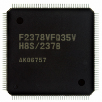
DF61657CN35FTV Renesas Electronics America, DF61657CN35FTV Datasheet - Page 353

DF61657CN35FTV
Manufacturer Part Number
DF61657CN35FTV
Description
IC H8SX/1657 MCU FLASH 120TQFP
Manufacturer
Renesas Electronics America
Series
H8® H8SX/1600r
Datasheet
1.DF61656N35FTV.pdf
(894 pages)
Specifications of DF61657CN35FTV
Core Processor
H8SX
Core Size
32-Bit
Speed
35MHz
Connectivity
SCI, SmartCard
Peripherals
DMA, PWM, WDT
Number Of I /o
82
Program Memory Size
768KB (768K x 8)
Program Memory Type
FLASH
Ram Size
24K x 8
Voltage - Supply (vcc/vdd)
3 V ~ 3.6 V
Data Converters
A/D 8x10b; D/A 2x8b
Oscillator Type
Internal
Operating Temperature
-20°C ~ 75°C
Package / Case
120-TQFP, 120-VQFP
For Use With
3DK1657 - DEV EVAL KIT FOR H8SX/1657
Lead Free Status / RoHS Status
Lead free / RoHS Compliant
Eeprom Size
-
Available stocks
Company
Part Number
Manufacturer
Quantity
Price
Company:
Part Number:
DF61657CN35FTV
Manufacturer:
RENESAS
Quantity:
101
Company:
Part Number:
DF61657CN35FTV
Manufacturer:
Renesas Electronics America
Quantity:
10 000
- Current page: 353 of 894
- Download datasheet (5Mb)
8.5.3
By specifying bit SM1 in MRA and bit DM1 in MRB to the fixed address mode, a part of transfer
information will not be written back. This function is performed regardless of short or full address
mode. Table 8.5 shows the transfer information writeback skip condition and writeback skipped
registers. Note that the CRA and CRB are always written back regardless of the short or full
address mode. In addition in full address mode, the writeback of the MRA and MRB are always
skipped.
Table 8.5
8.5.4
In normal transfer mode, one operation transfers one byte, one word, or one longword of data.
From 1 to 65,536 transfers can be specified. The transfer source and destination addresses can be
specified as incremented, decremented, or fixed. When the specified number of transfers ends, an
interrupt can be requested to the CPU.
Table 8.6 lists the register function in normal transfer mode. Figure 8.7 shows the memory map in
normal transfer mode.
Table 8.6
Note:
SM1
0
0
1
1
Register
SAR
DAR
CRA
CRB
*
Transfer Information Writeback Skip Function
Normal Transfer Mode
Transfer information writeback is skipped.
Transfer Information Writeback Skip Condition and Writeback Skipped
Registers
Register Function in Normal Transfer Mode
Function
Source address
Destination address
Transfer count A
Transfer count B
DM1
0
1
0
1
SAR
Skipped
Skipped
Written back
Written back
Written Back Value
Not updated
Incremented/decremented/fixed*
Incremented/decremented/fixed*
CRA − 1
Section 8 Data Transfer Controller (DTC)
Rev. 2.00 Jun. 28, 2007 Page 327 of 864
DAR
Skipped
Written back
Skipped
Written back
REJ09B0341-0200
Related parts for DF61657CN35FTV
Image
Part Number
Description
Manufacturer
Datasheet
Request
R

Part Number:
Description:
KIT STARTER FOR M16C/29
Manufacturer:
Renesas Electronics America
Datasheet:

Part Number:
Description:
KIT STARTER FOR R8C/2D
Manufacturer:
Renesas Electronics America
Datasheet:

Part Number:
Description:
R0K33062P STARTER KIT
Manufacturer:
Renesas Electronics America
Datasheet:

Part Number:
Description:
KIT STARTER FOR R8C/23 E8A
Manufacturer:
Renesas Electronics America
Datasheet:

Part Number:
Description:
KIT STARTER FOR R8C/25
Manufacturer:
Renesas Electronics America
Datasheet:

Part Number:
Description:
KIT STARTER H8S2456 SHARPE DSPLY
Manufacturer:
Renesas Electronics America
Datasheet:

Part Number:
Description:
KIT STARTER FOR R8C38C
Manufacturer:
Renesas Electronics America
Datasheet:

Part Number:
Description:
KIT STARTER FOR R8C35C
Manufacturer:
Renesas Electronics America
Datasheet:

Part Number:
Description:
KIT STARTER FOR R8CL3AC+LCD APPS
Manufacturer:
Renesas Electronics America
Datasheet:

Part Number:
Description:
KIT STARTER FOR RX610
Manufacturer:
Renesas Electronics America
Datasheet:

Part Number:
Description:
KIT STARTER FOR R32C/118
Manufacturer:
Renesas Electronics America
Datasheet:

Part Number:
Description:
KIT DEV RSK-R8C/26-29
Manufacturer:
Renesas Electronics America
Datasheet:

Part Number:
Description:
KIT STARTER FOR SH7124
Manufacturer:
Renesas Electronics America
Datasheet:

Part Number:
Description:
KIT STARTER FOR H8SX/1622
Manufacturer:
Renesas Electronics America
Datasheet:

Part Number:
Description:
KIT DEV FOR SH7203
Manufacturer:
Renesas Electronics America
Datasheet:


