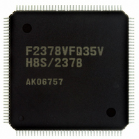
DF61657CN35FTV Renesas Electronics America, DF61657CN35FTV Datasheet - Page 301

DF61657CN35FTV
Manufacturer Part Number
DF61657CN35FTV
Description
IC H8SX/1657 MCU FLASH 120TQFP
Manufacturer
Renesas Electronics America
Series
H8® H8SX/1600r
Datasheet
1.DF61656N35FTV.pdf
(894 pages)
Specifications of DF61657CN35FTV
Core Processor
H8SX
Core Size
32-Bit
Speed
35MHz
Connectivity
SCI, SmartCard
Peripherals
DMA, PWM, WDT
Number Of I /o
82
Program Memory Size
768KB (768K x 8)
Program Memory Type
FLASH
Ram Size
24K x 8
Voltage - Supply (vcc/vdd)
3 V ~ 3.6 V
Data Converters
A/D 8x10b; D/A 2x8b
Oscillator Type
Internal
Operating Temperature
-20°C ~ 75°C
Package / Case
120-TQFP, 120-VQFP
For Use With
3DK1657 - DEV EVAL KIT FOR H8SX/1657
Lead Free Status / RoHS Status
Lead free / RoHS Compliant
Eeprom Size
-
Available stocks
Company
Part Number
Manufacturer
Quantity
Price
Company:
Part Number:
DF61657CN35FTV
Manufacturer:
RENESAS
Quantity:
101
Company:
Part Number:
DF61657CN35FTV
Manufacturer:
Renesas Electronics America
Quantity:
10 000
- Current page: 301 of 894
- Download datasheet (5Mb)
(2)
Figure 7.19 shows the XY conversion using the offset addition in repeat transfer mode.
In figure 7.19, the source address side is specified to the repeat area by DACR and the offset
addition is selected. The offset value is set to 4 × data access size (when the data access size is
longword, H'00000010 is set in DOFR, as an example). The repeat size is set to 4 × data access
size (when the data access size is longword, the repeat size is set to 4 × 4 = 16 bytes, as an
example). The increment or decrement by 1, 2, or 4 is specified as the transfer destination address.
A repeat size end interrupt is requested when the repeat size of transfers is completed.
When a transfer starts, the transfer source address is added to the offset every time data is
transferred. The transfer data is written to the destination continuous addresses. When data 4 is
transferred meaning that the repeat size of transfers is completed, the transfer source address
returns to the transfer start address (address of data 1 on the transfer source) and a repeat size end
interrupt is requested. While this interrupt stops the transfer temporarily, the contents of DSAR are
written to the address of data 5 by the CPU (when the data access size is longword, write the data
1 address + 4). When the DTE bit in DMDR is set to 1, the transfer is resumed from the state when
the transfer is stopped. Accordingly, operations are repeated and the transfer source data is
transposed to the destination area (XY conversion).
Offset
Offset
Offset
Figure 7.19 XY Conversion Operation Using Offset Addition in Repeat Transfer Mode
XY Conversion Using Offset
Data 1
Data 2
Data 3
Data 4
1st transfer
Data 1
Data 5
Data 9
Data 13
Data 2
Data 6
Data 10
Data 14
Data 3
Data 7
Data 11
Data 15
Data 4
Data 8
Data 12
Data 16
Data 5
Data 6
Data 7
Data 8
Interrupt
request
generated
Address
initialized
Data 9
Data 10
Data 11
Data 12
2nd transfer
Data 1
Data 5
Data 9
Data 13
Data 2
Data 6
Data 10
Data 14
Data 3
Data 7
Data 11
Data 15
Data 4
Data 8
Data 12
Data 16
Data 13
Data 14
Data 15
Data 16
Transfer source
addresses
changed
by CPU
Transfer
Interrupt
request
generated
Address
initialized
1st transfer
2nd transfer
3rd transfer
4th transfer
3rd transfer
Data 1
Data 5
Data 9
Data 13
Data 2
Data 6
Data 10
Data 14
Data 3
Data 7
Data 11
Data 15
Data 4
Data 8
Data 12
Data 16
Rev. 2.00 Jun. 28, 2007 Page 275 of 864
Data 1
Data 5
Data 13
Data 9
Transfer source
addresses
changed
by CPU
Interrupt
request
generated
Transfer
Section 7 DMA Controller (DMAC)
Data 2
Data 6
Data 10
Data 14
Data 1
Data 2
Data 3
Data 4
Data 5
Data 6
Data 7
Data 8
Data 9
Data 10
Data 11
Data 12
Data 13
Data 14
Data 15
Data 16
Data 3
Data 7
Data 11
Data 15
REJ09B0341-0200
Data 16
Data 4
Data 8
Data 12
1st transfer
2nd transfer
3rd transfer
4th transfer
Related parts for DF61657CN35FTV
Image
Part Number
Description
Manufacturer
Datasheet
Request
R

Part Number:
Description:
KIT STARTER FOR M16C/29
Manufacturer:
Renesas Electronics America
Datasheet:

Part Number:
Description:
KIT STARTER FOR R8C/2D
Manufacturer:
Renesas Electronics America
Datasheet:

Part Number:
Description:
R0K33062P STARTER KIT
Manufacturer:
Renesas Electronics America
Datasheet:

Part Number:
Description:
KIT STARTER FOR R8C/23 E8A
Manufacturer:
Renesas Electronics America
Datasheet:

Part Number:
Description:
KIT STARTER FOR R8C/25
Manufacturer:
Renesas Electronics America
Datasheet:

Part Number:
Description:
KIT STARTER H8S2456 SHARPE DSPLY
Manufacturer:
Renesas Electronics America
Datasheet:

Part Number:
Description:
KIT STARTER FOR R8C38C
Manufacturer:
Renesas Electronics America
Datasheet:

Part Number:
Description:
KIT STARTER FOR R8C35C
Manufacturer:
Renesas Electronics America
Datasheet:

Part Number:
Description:
KIT STARTER FOR R8CL3AC+LCD APPS
Manufacturer:
Renesas Electronics America
Datasheet:

Part Number:
Description:
KIT STARTER FOR RX610
Manufacturer:
Renesas Electronics America
Datasheet:

Part Number:
Description:
KIT STARTER FOR R32C/118
Manufacturer:
Renesas Electronics America
Datasheet:

Part Number:
Description:
KIT DEV RSK-R8C/26-29
Manufacturer:
Renesas Electronics America
Datasheet:

Part Number:
Description:
KIT STARTER FOR SH7124
Manufacturer:
Renesas Electronics America
Datasheet:

Part Number:
Description:
KIT STARTER FOR H8SX/1622
Manufacturer:
Renesas Electronics America
Datasheet:

Part Number:
Description:
KIT DEV FOR SH7203
Manufacturer:
Renesas Electronics America
Datasheet:


