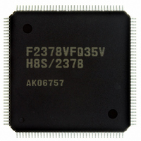
DF61657CN35FTV Renesas Electronics America, DF61657CN35FTV Datasheet - Page 325

DF61657CN35FTV
Manufacturer Part Number
DF61657CN35FTV
Description
IC H8SX/1657 MCU FLASH 120TQFP
Manufacturer
Renesas Electronics America
Series
H8® H8SX/1600r
Datasheet
1.DF61656N35FTV.pdf
(894 pages)
Specifications of DF61657CN35FTV
Core Processor
H8SX
Core Size
32-Bit
Speed
35MHz
Connectivity
SCI, SmartCard
Peripherals
DMA, PWM, WDT
Number Of I /o
82
Program Memory Size
768KB (768K x 8)
Program Memory Type
FLASH
Ram Size
24K x 8
Voltage - Supply (vcc/vdd)
3 V ~ 3.6 V
Data Converters
A/D 8x10b; D/A 2x8b
Oscillator Type
Internal
Operating Temperature
-20°C ~ 75°C
Package / Case
120-TQFP, 120-VQFP
For Use With
3DK1657 - DEV EVAL KIT FOR H8SX/1657
Lead Free Status / RoHS Status
Lead free / RoHS Compliant
Eeprom Size
-
Available stocks
Company
Part Number
Manufacturer
Quantity
Price
Company:
Part Number:
DF61657CN35FTV
Manufacturer:
RENESAS
Quantity:
101
Company:
Part Number:
DF61657CN35FTV
Manufacturer:
Renesas Electronics America
Quantity:
10 000
- Current page: 325 of 894
- Download datasheet (5Mb)
(4)
When an overflow on the extended repeat area occurs while the extended repeat area is specified
and the SARIE or DARIE bit in DACR is set to 1, an interrupt by an extended repeat area
overflow is requested. When the interrupt is requested, the DMA transfer is terminated, the DTE
bit in DMDR is cleared to 0, and the ESIF bit in DMDR is set to 1.
In dual address mode, even if an interrupt by an extended repeat area overflow occurs during a
read cycle, the following write cycle is performed.
In block transfer mode, even if an interrupt by an extended repeat area overflow occurs during a 1-
block transfer, the remaining data is transferred. The transfer is not terminated by an extended
repeat area overflow interrupt unless the current transfer is complete.
(5)
When the DTE bit in DMDR is cleared to 0 by the CPU, a transfer is completed after the current
DMA cycle and a DMA cycle in which the transfer request is accepted are completed.
In block transfer mode, a DMA transfer is completed after 1-block data is transferred.
(6)
When an NMI interrupt is requested, the DTE bits for all the channels are cleared to 0 and the
ERRF bit in DMDR_0 is set to 1. When an NMI interrupt is requested during a DMA transfer, the
transfer is forced to stop. To perform DMA transfer after an NMI interrupt is requested, clear the
ERRF bit to 0 and then set the DTE bits for the channels to 1.
The transfer end timings after an NMI interrupt is requested are shown below.
(a)
In dual address mode, a DMA transfer is completed after completion of the write cycle for one
transfer unit.
In single address mode, a DMA transfer is completed after completion of the bus cycle for one
transfer unit.
(b) Block Transfer Mode
A DMA transfer is forced to stop. Since a 1-block size of transfers is not completed, operation is
not guaranteed.
In dual address mode, the write cycle corresponding to the read cycle is performed. This is similar
to (a) in normal transfer mode.
Transfer End by Interrupt on Extended Repeat Area Overflow
Transfer End by Clearing DTE Bit in DMDR
Transfer End by NMI Interrupt
Normal Transfer Mode and Repeat Transfer Mode
Rev. 2.00 Jun. 28, 2007 Page 299 of 864
Section 7 DMA Controller (DMAC)
REJ09B0341-0200
Related parts for DF61657CN35FTV
Image
Part Number
Description
Manufacturer
Datasheet
Request
R

Part Number:
Description:
KIT STARTER FOR M16C/29
Manufacturer:
Renesas Electronics America
Datasheet:

Part Number:
Description:
KIT STARTER FOR R8C/2D
Manufacturer:
Renesas Electronics America
Datasheet:

Part Number:
Description:
R0K33062P STARTER KIT
Manufacturer:
Renesas Electronics America
Datasheet:

Part Number:
Description:
KIT STARTER FOR R8C/23 E8A
Manufacturer:
Renesas Electronics America
Datasheet:

Part Number:
Description:
KIT STARTER FOR R8C/25
Manufacturer:
Renesas Electronics America
Datasheet:

Part Number:
Description:
KIT STARTER H8S2456 SHARPE DSPLY
Manufacturer:
Renesas Electronics America
Datasheet:

Part Number:
Description:
KIT STARTER FOR R8C38C
Manufacturer:
Renesas Electronics America
Datasheet:

Part Number:
Description:
KIT STARTER FOR R8C35C
Manufacturer:
Renesas Electronics America
Datasheet:

Part Number:
Description:
KIT STARTER FOR R8CL3AC+LCD APPS
Manufacturer:
Renesas Electronics America
Datasheet:

Part Number:
Description:
KIT STARTER FOR RX610
Manufacturer:
Renesas Electronics America
Datasheet:

Part Number:
Description:
KIT STARTER FOR R32C/118
Manufacturer:
Renesas Electronics America
Datasheet:

Part Number:
Description:
KIT DEV RSK-R8C/26-29
Manufacturer:
Renesas Electronics America
Datasheet:

Part Number:
Description:
KIT STARTER FOR SH7124
Manufacturer:
Renesas Electronics America
Datasheet:

Part Number:
Description:
KIT STARTER FOR H8SX/1622
Manufacturer:
Renesas Electronics America
Datasheet:

Part Number:
Description:
KIT DEV FOR SH7203
Manufacturer:
Renesas Electronics America
Datasheet:


