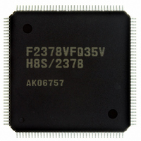
DF61657CN35FTV Renesas Electronics America, DF61657CN35FTV Datasheet - Page 318

DF61657CN35FTV
Manufacturer Part Number
DF61657CN35FTV
Description
IC H8SX/1657 MCU FLASH 120TQFP
Manufacturer
Renesas Electronics America
Series
H8® H8SX/1600r
Datasheet
1.DF61656N35FTV.pdf
(894 pages)
Specifications of DF61657CN35FTV
Core Processor
H8SX
Core Size
32-Bit
Speed
35MHz
Connectivity
SCI, SmartCard
Peripherals
DMA, PWM, WDT
Number Of I /o
82
Program Memory Size
768KB (768K x 8)
Program Memory Type
FLASH
Ram Size
24K x 8
Voltage - Supply (vcc/vdd)
3 V ~ 3.6 V
Data Converters
A/D 8x10b; D/A 2x8b
Oscillator Type
Internal
Operating Temperature
-20°C ~ 75°C
Package / Case
120-TQFP, 120-VQFP
For Use With
3DK1657 - DEV EVAL KIT FOR H8SX/1657
Lead Free Status / RoHS Status
Lead free / RoHS Compliant
Eeprom Size
-
Available stocks
Company
Part Number
Manufacturer
Quantity
Price
Company:
Part Number:
DF61657CN35FTV
Manufacturer:
RENESAS
Quantity:
101
Company:
Part Number:
DF61657CN35FTV
Manufacturer:
Renesas Electronics America
Quantity:
10 000
- Current page: 318 of 894
- Download datasheet (5Mb)
Section 7 DMA Controller (DMAC)
(6)
When the NRD bit in DMDR is set to 1, the timing of receiving the next transfer request is
delayed for one cycle.
Figure 7.33 shows an example of normal transfer mode activated by the DREQ signal low level
with NRD = 1.
The DREQ signal is sampled every cycle from the next rising edge of the Bφ signal immediately
after the DTE bit write cycle.
When a low level of the DREQ signal is detected while a transfer request by the DREQ signal is
enabled, a transfer request is held in the DMAC. When the DMAC is activated, the transfer
request is cleared. Receiving the next transfer request resumes after completion of the write cycle
and then a low level of the DREQ signal is detected. This operation is repeated until the transfer is
completed.
Bφ
DREQ
Address bus
Channel
Rev. 2.00 Jun. 28, 2007 Page 292 of 864
REJ09B0341-0200
[1]
[2][5] The DMAC is activated and the transfer request is cleared.
[3][6] A DMA cycle is started.
[4][7] Transfer request enable is resumed one cycle after completion of the write cycle.
Activation Timing by DREQ Low Level with NRD = 1
After DMA transfer request is enabled, a low level of the DREQ signal is detected at the rising edge of the Bφ signal and a transfer
request is held.
(A low level of the DREQ signal is detected at the rising edge of the Bφ signal and a transfer request is held. This is the same as [1].)
Figure 7.33 Example of Transfer in Normal Transfer Mode Activated
[1]
Request
Bus released
Min. of 3 cycles
[2]
Duration of transfer
[3]
request disabled
DMA read
by DREQ Low Level with NRD = 1
cycle
Transfer
source
DMA read
destination
Transfer
Duration of transfer request
cycle
disabled which is extended
Transfer request enable resumed
by NRD
Bus released
[4]
Request
Min. of 3 cycles
[5]
[6]
Duration of transfer
request disabled
DMA read
Transfer
source
cycle
Transfer request enable resumed
DMA read
destination
cycle
Transfer
Duration of transfer request
disabled which is extended
by NRD
Bus released
[7]
Related parts for DF61657CN35FTV
Image
Part Number
Description
Manufacturer
Datasheet
Request
R

Part Number:
Description:
KIT STARTER FOR M16C/29
Manufacturer:
Renesas Electronics America
Datasheet:

Part Number:
Description:
KIT STARTER FOR R8C/2D
Manufacturer:
Renesas Electronics America
Datasheet:

Part Number:
Description:
R0K33062P STARTER KIT
Manufacturer:
Renesas Electronics America
Datasheet:

Part Number:
Description:
KIT STARTER FOR R8C/23 E8A
Manufacturer:
Renesas Electronics America
Datasheet:

Part Number:
Description:
KIT STARTER FOR R8C/25
Manufacturer:
Renesas Electronics America
Datasheet:

Part Number:
Description:
KIT STARTER H8S2456 SHARPE DSPLY
Manufacturer:
Renesas Electronics America
Datasheet:

Part Number:
Description:
KIT STARTER FOR R8C38C
Manufacturer:
Renesas Electronics America
Datasheet:

Part Number:
Description:
KIT STARTER FOR R8C35C
Manufacturer:
Renesas Electronics America
Datasheet:

Part Number:
Description:
KIT STARTER FOR R8CL3AC+LCD APPS
Manufacturer:
Renesas Electronics America
Datasheet:

Part Number:
Description:
KIT STARTER FOR RX610
Manufacturer:
Renesas Electronics America
Datasheet:

Part Number:
Description:
KIT STARTER FOR R32C/118
Manufacturer:
Renesas Electronics America
Datasheet:

Part Number:
Description:
KIT DEV RSK-R8C/26-29
Manufacturer:
Renesas Electronics America
Datasheet:

Part Number:
Description:
KIT STARTER FOR SH7124
Manufacturer:
Renesas Electronics America
Datasheet:

Part Number:
Description:
KIT STARTER FOR H8SX/1622
Manufacturer:
Renesas Electronics America
Datasheet:

Part Number:
Description:
KIT DEV FOR SH7203
Manufacturer:
Renesas Electronics America
Datasheet:


