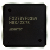
DF61657CN35FTV Renesas Electronics America, DF61657CN35FTV Datasheet - Page 717

DF61657CN35FTV
Manufacturer Part Number
DF61657CN35FTV
Description
IC H8SX/1657 MCU FLASH 120TQFP
Manufacturer
Renesas Electronics America
Series
H8® H8SX/1600r
Datasheet
1.DF61656N35FTV.pdf
(894 pages)
Specifications of DF61657CN35FTV
Core Processor
H8SX
Core Size
32-Bit
Speed
35MHz
Connectivity
SCI, SmartCard
Peripherals
DMA, PWM, WDT
Number Of I /o
82
Program Memory Size
768KB (768K x 8)
Program Memory Type
FLASH
Ram Size
24K x 8
Voltage - Supply (vcc/vdd)
3 V ~ 3.6 V
Data Converters
A/D 8x10b; D/A 2x8b
Oscillator Type
Internal
Operating Temperature
-20°C ~ 75°C
Package / Case
120-TQFP, 120-VQFP
For Use With
3DK1657 - DEV EVAL KIT FOR H8SX/1657
Lead Free Status / RoHS Status
Lead free / RoHS Compliant
Eeprom Size
-
Available stocks
Company
Part Number
Manufacturer
Quantity
Price
Company:
Part Number:
DF61657CN35FTV
Manufacturer:
RENESAS
Quantity:
101
Company:
Part Number:
DF61657CN35FTV
Manufacturer:
Renesas Electronics America
Quantity:
10 000
- Current page: 717 of 894
- Download datasheet (5Mb)
12. Programming is executed. The entry point of the programming program is at the address which
13. The return value in the programming program, the FPFR parameter is determined.
14. Determine whether programming of the necessary data has finished. If more than 128 bytes of
15. Programming end processing is executed.
Example of FMPDR parameter setting: When the storage destination for the program data
is 16 bytes after #DLTOP (start address of the download destination specified by FTDAR).
Call the subroutine to execute programming by using the following steps.
MOV.L
JSR
NOP
The general registers other than ER0 and ER1 are held in the programming program.
R0L is a return value of the FPFR parameter.
Since the stack area is used in the programming program, a stack area of 128 bytes at the
data are to be programmed, update the FMPAR and FMPDR parameters in 128-byte units, and
repeat steps 11 to 14. Increment the programming destination address by 128 bytes and update
the programming data pointer correctly. If an address which has already been programmed is
written to again, not only will a programming error occur, but also flash memory will be
damaged.
The entry point of the programming library is at the address which is 16 bytes after the start
address of the download destination specified by FTDAR. Call the subroutine by using the
following steps.
MOV.L
MOV.L
MOV.L
JSR
The general registers other than ER0 and ER1 are held in the programming end program.
R0L is a return value of the FPFR parameter.
Since the stack area is used in the programming end program, a stack area of 128 bytes at
is flash memory, even if the programming routine is executed, programming is not
executed and an error is returned to the FPFR parameter. In this case, the program data
must be transferred to the on-chip RAM and then programming must be executed.
maximum must be allocated in RAM.
the maximum must be allocated in RAM.
#DLTOP+16,ER2
@ER2
#H'F0F0F0F0,ER0
#H'0F0F0F0F,ER1
#DLTOP+16,ER2
@ER2
; Set entry address to ER2
; Call programming routine
; Set entry address to ER2
; Call programming end routine
Section 18 Flash Memory (0.18-µm F-ZTAT Version)
Rev. 2.00 Jun. 28, 2007 Page 691 of 864
REJ09B0341-0200
Related parts for DF61657CN35FTV
Image
Part Number
Description
Manufacturer
Datasheet
Request
R

Part Number:
Description:
KIT STARTER FOR M16C/29
Manufacturer:
Renesas Electronics America
Datasheet:

Part Number:
Description:
KIT STARTER FOR R8C/2D
Manufacturer:
Renesas Electronics America
Datasheet:

Part Number:
Description:
R0K33062P STARTER KIT
Manufacturer:
Renesas Electronics America
Datasheet:

Part Number:
Description:
KIT STARTER FOR R8C/23 E8A
Manufacturer:
Renesas Electronics America
Datasheet:

Part Number:
Description:
KIT STARTER FOR R8C/25
Manufacturer:
Renesas Electronics America
Datasheet:

Part Number:
Description:
KIT STARTER H8S2456 SHARPE DSPLY
Manufacturer:
Renesas Electronics America
Datasheet:

Part Number:
Description:
KIT STARTER FOR R8C38C
Manufacturer:
Renesas Electronics America
Datasheet:

Part Number:
Description:
KIT STARTER FOR R8C35C
Manufacturer:
Renesas Electronics America
Datasheet:

Part Number:
Description:
KIT STARTER FOR R8CL3AC+LCD APPS
Manufacturer:
Renesas Electronics America
Datasheet:

Part Number:
Description:
KIT STARTER FOR RX610
Manufacturer:
Renesas Electronics America
Datasheet:

Part Number:
Description:
KIT STARTER FOR R32C/118
Manufacturer:
Renesas Electronics America
Datasheet:

Part Number:
Description:
KIT DEV RSK-R8C/26-29
Manufacturer:
Renesas Electronics America
Datasheet:

Part Number:
Description:
KIT STARTER FOR SH7124
Manufacturer:
Renesas Electronics America
Datasheet:

Part Number:
Description:
KIT STARTER FOR H8SX/1622
Manufacturer:
Renesas Electronics America
Datasheet:

Part Number:
Description:
KIT DEV FOR SH7203
Manufacturer:
Renesas Electronics America
Datasheet:


