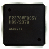
DF61657CN35FTV Renesas Electronics America, DF61657CN35FTV Datasheet - Page 585

DF61657CN35FTV
Manufacturer Part Number
DF61657CN35FTV
Description
IC H8SX/1657 MCU FLASH 120TQFP
Manufacturer
Renesas Electronics America
Series
H8® H8SX/1600r
Datasheet
1.DF61656N35FTV.pdf
(894 pages)
Specifications of DF61657CN35FTV
Core Processor
H8SX
Core Size
32-Bit
Speed
35MHz
Connectivity
SCI, SmartCard
Peripherals
DMA, PWM, WDT
Number Of I /o
82
Program Memory Size
768KB (768K x 8)
Program Memory Type
FLASH
Ram Size
24K x 8
Voltage - Supply (vcc/vdd)
3 V ~ 3.6 V
Data Converters
A/D 8x10b; D/A 2x8b
Oscillator Type
Internal
Operating Temperature
-20°C ~ 75°C
Package / Case
120-TQFP, 120-VQFP
For Use With
3DK1657 - DEV EVAL KIT FOR H8SX/1657
Lead Free Status / RoHS Status
Lead free / RoHS Compliant
Eeprom Size
-
Available stocks
Company
Part Number
Manufacturer
Quantity
Price
Company:
Part Number:
DF61657CN35FTV
Manufacturer:
RENESAS
Quantity:
101
Company:
Part Number:
DF61657CN35FTV
Manufacturer:
Renesas Electronics America
Quantity:
10 000
- Current page: 585 of 894
- Download datasheet (5Mb)
Note:
Bit
6
5
4
3
2
1
0
etu (Elementary Time Unit): 1-bit transfer time
Bit Name
BLK
PE
O/E
BCP1
BCP0
CKS1
CKS0
Initial
Value
0
0
0
0
0
0
0
R/W
R/W
R/W
R/W
R/W
R/W
R/W
R/W
Description
Setting this bit to 1 allows block transfer mode operation.
For details, see section 14.7.3, Block Transfer Mode.
Parity Enable (valid only in asynchronous mode)
When this bit is set to 1, the parity bit is added to transmit
data before transmission, and the parity bit is checked in
reception. Set this bit to 1 in smart card interface mode.
Parity Mode (valid only when the PE bit is 1 in
asynchronous mode)
0: Selects even parity
1: Selects odd parity
For details on the usage of this bit in smart card interface
mode, see section 14.7.2, Data Format (Except in Block
Transfer Mode).
Basic Clock Pulse 1,0
These bits select the number of basic clock cycles in a 1-
bit data transfer time in smart card interface mode.
00: 32 clock cycles (S = 32)
01: 64 clock cycles (S = 64)
10: 372 clock cycles (S = 372)
11: 256 clock cycles (S = 256)
For details, see section 14.7.4, Receive Data Sampling
Timing and Reception Margin. S is described in section
14.3.9, Bit Rate Register (BRR).
Clock Select 1,0
These bits select the clock source for the baud rate
generator.
00: Pφ clock (n = 0)
01: Pφ/4 clock (n = 1)
10: Pφ/16 clock (n = 2)
11: Pφ/64 clock (n = 3)
For the relation between the settings of these bits and the
baud rate, see section 14.3.9, Bit Rate Register (BRR). n
is the decimal display of the value of n in BRR (see
section 14.3.9, Bit Rate Register (BRR)).
Section 14 Serial Communication Interface (SCI)
Rev. 2.00 Jun. 28, 2007 Page 559 of 864
REJ09B0341-0200
Related parts for DF61657CN35FTV
Image
Part Number
Description
Manufacturer
Datasheet
Request
R

Part Number:
Description:
KIT STARTER FOR M16C/29
Manufacturer:
Renesas Electronics America
Datasheet:

Part Number:
Description:
KIT STARTER FOR R8C/2D
Manufacturer:
Renesas Electronics America
Datasheet:

Part Number:
Description:
R0K33062P STARTER KIT
Manufacturer:
Renesas Electronics America
Datasheet:

Part Number:
Description:
KIT STARTER FOR R8C/23 E8A
Manufacturer:
Renesas Electronics America
Datasheet:

Part Number:
Description:
KIT STARTER FOR R8C/25
Manufacturer:
Renesas Electronics America
Datasheet:

Part Number:
Description:
KIT STARTER H8S2456 SHARPE DSPLY
Manufacturer:
Renesas Electronics America
Datasheet:

Part Number:
Description:
KIT STARTER FOR R8C38C
Manufacturer:
Renesas Electronics America
Datasheet:

Part Number:
Description:
KIT STARTER FOR R8C35C
Manufacturer:
Renesas Electronics America
Datasheet:

Part Number:
Description:
KIT STARTER FOR R8CL3AC+LCD APPS
Manufacturer:
Renesas Electronics America
Datasheet:

Part Number:
Description:
KIT STARTER FOR RX610
Manufacturer:
Renesas Electronics America
Datasheet:

Part Number:
Description:
KIT STARTER FOR R32C/118
Manufacturer:
Renesas Electronics America
Datasheet:

Part Number:
Description:
KIT DEV RSK-R8C/26-29
Manufacturer:
Renesas Electronics America
Datasheet:

Part Number:
Description:
KIT STARTER FOR SH7124
Manufacturer:
Renesas Electronics America
Datasheet:

Part Number:
Description:
KIT STARTER FOR H8SX/1622
Manufacturer:
Renesas Electronics America
Datasheet:

Part Number:
Description:
KIT DEV FOR SH7203
Manufacturer:
Renesas Electronics America
Datasheet:


