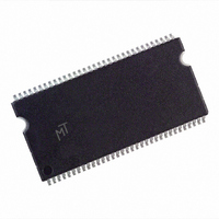
MT46V32M4TG-6T:D TR Micron Technology Inc, MT46V32M4TG-6T:D TR Datasheet - Page 83

MT46V32M4TG-6T:D TR
Manufacturer Part Number
MT46V32M4TG-6T:D TR
Description
IC DDR SDRAM 128MBIT 6NS 66TSOP
Manufacturer
Micron Technology Inc
Datasheet
1.MT46V32M4TG-6TD_TR.pdf
(93 pages)
Specifications of MT46V32M4TG-6T:D TR
Format - Memory
RAM
Memory Type
DDR SDRAM
Memory Size
128M (32Mx4)
Speed
6ns
Interface
Parallel
Voltage - Supply
2.3 V ~ 2.7 V
Operating Temperature
0°C ~ 70°C
Package / Case
66-TSOP
Lead Free Status / RoHS Status
Contains lead / RoHS non-compliant
Other names
557-1024-2
Timing Diagrams
Figure 45:
09005aef8074a655
128MBDDRx4x8x16_2.fm - Rev. J 4/05 EN
COMMAND
BA0, BA1
A0-A9,
V
A11
DQS
V
CK#
CKE
A10
V
DM
DD
V
DQ
CK
TT
REF
DD
6
Q
1
t
VTD
Initialize and Load Mode Registers
1
LVCMOS
LOW LEVEL
T = 200µs
Power-up: V
Notes: 1. V
(
(
(
(
(
(
(
(
(
(
)
(
(
)
(
)
(
)
(
)
(
)
(
(
(
)
)
)
)
)
)
)
)
)
)
)
)
)
2. Reset the DLL with A8 = H while programming the operating parameters.
3.
4. The two AUTO REFRESH commands at Td0 and Te0 may be applied following the LOAD
5. Although not required by the Micron device, JEDEC specifies issuing another LMR com-
6. PRE = PRECHARGE command, LMR = LOAD MODE REGISTER command, AR = AUTO
(
(
(
(
(
(
(
(
(
(
(
)
(
)
(
)
(
)
(
)
(
)
(
(
(
)
)
)
)
)
)
)
)
)
)
)
)
)
DD
and CK stable
zero to avoid device latch-up. V
0.3V. Alternatively, V
provided a minimum of 42 ohms of series resistance is used between the V
the input pin. Once initialized, inclding during self refresh mode, V
powered within specified range.
t
before a READ command can be issued.
MODE REGISTER (LMR) command at Ta0.
mand (A8 = L) prior to activating any bank. If another command is issued, the same operat-
ing parmeters previously issued must be used.
REFRESH command, ACT = ACTIVE command, RA = Row Address, BA = Bank Address.
t IS
t
MRD is required before any command can be applied, and 200 cycles of CK are required
IS
TT
T0
NOP
High-Z
High-Z
t IH
t
is not applied directly to the device; however,
t
IH
CH
t
CK
t
CL
ALL BANKS
t IS
PRE
T1
t IH
(
(
(
(
(
(
(
(
(
(
)
(
)
(
)
(
)
(
)
(
)
(
)
)
)
t RP
)
)
)
)
)
)
)
(
(
(
(
(
(
(
(
(
(
)
(
)
(
)
(
)
(
)
(
)
(
)
)
)
Load Extended
)
)
)
)
)
)
)
Mode Register
TT
t IS
t IS
t IS
BA0 = H,
may be 1.35V maximum during power up, even if V
BA1 = L
CODE
CODE
LMR
Ta0
t IH
t IH
t IH
83
t MRD
(
(
(
(
(
(
(
(
(
)
)
(
)
(
)
(
)
(
)
(
)
(
)
(
)
)
)
)
)
)
)
)
(
(
(
(
(
(
(
(
(
)
)
(
)
(
)
(
)
(
)
(
)
(
)
(
)
)
)
)
)
)
)
)
DD
Load Mode
Register
Q, V
BA0 = L,
BA1 = L
CODE
CODE
LMR
Tb0
Micron Technology, Inc., reserves the right to change products or specifications without notice.
TT
2
t MRD
, and V
(
(
(
(
(
(
(
)
)
)
)
)
)
)
(
(
(
(
(
(
(
(
(
)
)
)
)
)
)
)
)
)
(
(
(
(
(
(
(
(
)
(
)
(
)
(
)
(
)
(
)
(
)
(
(
)
)
)
)
)
)
)
)
)
ALL BANKS
t
IS
128Mb: x4, x8, x16 DDR SDRAM
Tc0
PRE
200 cycles of CK
REF
t
IH
t
t RP
, must be equal to or less than V
VTD should be greater than or equal to
(
(
(
(
(
(
(
(
)
(
)
(
)
(
)
(
)
(
)
(
)
(
(
)
)
)
)
)
)
)
)
)
(
(
(
(
(
(
(
(
)
(
)
(
)
(
)
(
)
(
)
(
)
(
(
)
)
)
)
)
)
)
)
)
Td0
3
AR
t RFC
©2000 Micron Technology, Inc. All rights reserved.
(
(
(
(
(
(
(
(
)
(
)
(
)
(
)
(
)
(
)
(
)
(
(
)
)
)
)
)
)
)
)
)
(
(
(
(
(
(
(
)
)
)
)
)
)
)
(
(
(
(
(
(
(
(
(
)
)
)
)
)
)
)
)
)
Timing Diagrams
REF
Te0
AR
must always be
t RFC
DD
TT
(
(
(
(
(
(
(
(
)
(
)
(
)
(
)
(
)
(
)
(
)
(
(
)
)
)
)
)
)
)
)
)
(
(
(
(
(
(
(
(
)
(
)
(
)
(
)
(
)
(
)
(
)
(
(
)
)
)
)
)
)
)
)
)
/V
5
supply and
DD
ACT 5
Tf0
RA
DON’T CARE
RA
BA
Q are 0V,
DD
+


