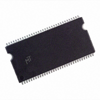
MT46V32M4TG-6T:D TR Micron Technology Inc, MT46V32M4TG-6T:D TR Datasheet - Page 14

MT46V32M4TG-6T:D TR
Manufacturer Part Number
MT46V32M4TG-6T:D TR
Description
IC DDR SDRAM 128MBIT 6NS 66TSOP
Manufacturer
Micron Technology Inc
Datasheet
1.MT46V32M4TG-6TD_TR.pdf
(93 pages)
Specifications of MT46V32M4TG-6T:D TR
Format - Memory
RAM
Memory Type
DDR SDRAM
Memory Size
128M (32Mx4)
Speed
6ns
Interface
Parallel
Voltage - Supply
2.3 V ~ 2.7 V
Operating Temperature
0°C ~ 70°C
Package / Case
66-TSOP
Lead Free Status / RoHS Status
Contains lead / RoHS non-compliant
Other names
557-1024-2
Functional Description
Initialization
09005aef8074a655
128MBDDRx4x8x16_2.fm - Rev. J 4/05 EN
The 128Mb DDR SDRAM is a high-speed CMOS, dynamic random-access memory con-
taining 134,217,728 bits. The 128Mb DDR SDRAM is internally configured as a quad-
bank DRAM.
The 128Mb DDR SDRAM uses a double data rate architecture to achieve high-speed
operation. The double data rate architecture is essentially a 2n-prefetch architecture,
with an interface designed to transfer two data words per clock cycle at the I/O pins. A
single read or write access for the 128Mb DDR SDRAM consists of a single 2n-bit wide,
one-clock-cycle data transfer at the internal DRAM core and two corresponding n-bit
wide, one-half-clock-cycle data transfers at the I/O pins.
Read and write accesses to the DDR SDRAM are burst oriented; accesses start at a
selected location and continue for a programmed number of locations in a programmed
sequence. Accesses begin with the registration of an ACTIVE command, which is then
followed by a READ or WRITE command. The address bits registered coincident with the
ACTIVE command are used to select the bank and row to be accessed (BA0, BA1 select
the bank; A0-A11 select the row). The address bits registered coincident with the READ
or WRITE command are used to select the starting column location for the burst access.
Prior to normal operation, the DDR SDRAM must be initialized. The following sections
provide detailed information covering device initialization, register definition, com-
mand descriptions, and device operation.
DDR SDRAMs must be powered up and initialized in a predefined manner. Operational
procedures other than those specified may result in undefined operation. Power must
first be applied to V
V
nent damage to the device. VREF can be applied any time after V
be nominally coincident with V
until after V
after V
and remain as such until power is cycled. Maintaining an LVCMOS LOW level on CKE
during power-up is required to ensure that the DQ and DQS outputs will be in the High-
Z state, where they will remain until driven in normal operation (by a read access). After
all power supply and reference voltages are stable, and the clock is stable, the DDR
SDRAM requires a 200µs delay prior to applying an executable command.
Once the 200µs delay has been satisfied, a DESELECT or NOP command should be
applied, and CKE should be brought HIGH. Following the NOP command, a PRE-
CHARGE ALL command should be applied. Next a LOAD MODE REGISTER command
should be issued for the extended mode register (BA1 LOW and BA0 HIGH) to enable the
DLL, followed by another LOAD MODE REGISTER command to the mode register (BA0/
BA1 both LOW) to reset the DLL and to program the operating parameters. Two-hun-
dred clock cycles are required between the DLL reset and any READ command. A PRE-
CHARGE ALL command should then be applied, placing the device in the all banks idle
state.
Once in the idle state, two AUTO REFRESH cycles must be performed (
isfied.) Additionally, a LOAD MODE REGISTER command for the mode register with the
reset DLL bit deactivated (i.e., to program operating parameters without resetting the
DLL) is required. Following these requirements, the DDR SDRAM is ready for normal
operation.
TT
). V
DD
TT
must be applied after V
is applied. After CKE passes through V
REF
is applied. CKE is an SSTL_2 input but will detect an LVCMOS LOW level
DD
and V
DD
14
Q simultaneously, and then to VREF (and to the system
TT
DD
. Except for CKE, inputs are not recognized as valid
Q to avoid device latch-up, which may cause perma-
Micron Technology, Inc., reserves the right to change products or specifications without notice.
128Mb: x4, x8, x16 DDR SDRAM
IH
, it will transition to a SSTL 2 signal
Functional Description
©2000 Micron Technology, Inc. All rights reserved.
DD
Q but is expected to
t
RFC must be sat-


