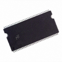
MT46V32M4TG-6T:D TR Micron Technology Inc, MT46V32M4TG-6T:D TR Datasheet - Page 26

MT46V32M4TG-6T:D TR
Manufacturer Part Number
MT46V32M4TG-6T:D TR
Description
IC DDR SDRAM 128MBIT 6NS 66TSOP
Manufacturer
Micron Technology Inc
Datasheet
1.MT46V32M4TG-6TD_TR.pdf
(93 pages)
Specifications of MT46V32M4TG-6T:D TR
Format - Memory
RAM
Memory Type
DDR SDRAM
Memory Size
128M (32Mx4)
Speed
6ns
Interface
Parallel
Voltage - Supply
2.3 V ~ 2.7 V
Operating Temperature
0°C ~ 70°C
Package / Case
66-TSOP
Lead Free Status / RoHS Status
Contains lead / RoHS non-compliant
Other names
557-1024-2
Figure 11:
READs
09005aef8074a655
128MBDDRx4x8x16_2.fm - Rev. J 4/05 EN
COMMAND
BA0, BA1
A0-A11
CK#
CK
Example: Meeting
Bank x
Row
ACT
T0
Note:
READ bursts are initiated with a READ command, as shown in Figure 12 on page 27.
The starting column and bank addresses are provided with the READ command and
auto precharge is either enabled or disabled for that burst access. If auto precharge is
enabled, the row being accessed is precharged at the completion of the burst.
During READ bursts, the valid data-out element from the starting column address will
be available following the CAS latency after the READ command. Each subsequent data-
out element will be valid nominally at the next positive or negative clock edge (i.e., at the
next crossing of CK and CK#). Figure 13 on page 28 shows general timing for each possi-
ble CAS latency setting. DQS is driven by the DDR SDRAM along with output data. The
initial LOW state on DQS is known as the read preamble; the LOW state coincident with
the last data-out element is known as the read postamble.
Upon completion of a burst, assuming no other commands have been initiated, the DQs
will go High-Z. A detailed explanation of
window hold), the valid data window are depicted in Figure 40 on page 77 and Figure 41
on page 78. A detailed explanation of
(data-out transition skew to CK) is depicted in Figure 42 on page 79.
Data from any READ burst may be concatenated with or truncated with data from a sub-
sequent READ command. In either case, a continuous flow of data can be maintained.
The first data element from the new burst follows either the last element of a completed
burst or the last desired data element of a longer burst which is being truncated. The
new READ command should be issued x cycles after the first READ command, where x
equals the number of desired data element pairs (pairs are required by the 2n-prefetch
architecture). This is shown in Figure 14 on page 29. A READ command can be initiated
on any clock cycle following a previous READ command. Nonconsecutive read data is
shown for illustration in Figure 15 on page 30. Full-speed random read accesses within a
page (or pages) can be performed as shown in Figure 16 on page 31.
NOP
For the READ commands used in the following illustrations, auto precharge is dis-
abled.
T1
t
RRD
t
RCD (
NOP
t
RRD) MIN When 2 <
T2
Row
Bank y
ACT
26
T3
t
DQSCK (DQS transition skew to CK) and
Micron Technology, Inc., reserves the right to change products or specifications without notice.
t
RCD (
t
DQSQ (valid data-out skew),
T4
NOP
t
128Mb: x4, x8, x16 DDR SDRAM
RRD) MIN/
t RCD
NOP
T5
t
CK≤3
©2000 Micron Technology, Inc. All rights reserved.
RD/WR
Bank y
T6
Col
t
QH (data-out
Operations
DON’T CARE
t
AC
T7
NOP


