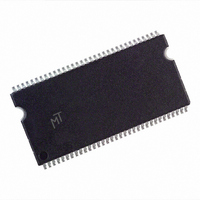
MT46V32M4TG-6T:D TR Micron Technology Inc, MT46V32M4TG-6T:D TR Datasheet - Page 71

MT46V32M4TG-6T:D TR
Manufacturer Part Number
MT46V32M4TG-6T:D TR
Description
IC DDR SDRAM 128MBIT 6NS 66TSOP
Manufacturer
Micron Technology Inc
Datasheet
1.MT46V32M4TG-6TD_TR.pdf
(93 pages)
Specifications of MT46V32M4TG-6T:D TR
Format - Memory
RAM
Memory Type
DDR SDRAM
Memory Size
128M (32Mx4)
Speed
6ns
Interface
Parallel
Voltage - Supply
2.3 V ~ 2.7 V
Operating Temperature
0°C ~ 70°C
Package / Case
66-TSOP
Lead Free Status / RoHS Status
Contains lead / RoHS non-compliant
Other names
557-1024-2
Figure 35:
09005aef8074a655
128MBDDRx4x8x16_2.fm - Rev. J 4/05 EN
a. The full variation in driver pull-down current from minimum to maximum process, temperature and volt-
age will lie within the outer bounding lines of the V-I curve of Figure 36
3.8
3.6
3.4
3.2
3.0
2.8
2.6
2.4
2.2
2.0
1.8
Derating Data Valid Window (
50/50
3.750
2.500
3.400
—— -75 @
—— -8 @
—— -75 @
—— -8 @
49.5/50.5
3.700
10. READs and WRITEs with auto precharge are not allowed to be issued until
11. Any positive glitch must be less than 1/3 of the clock cycle and not more than +400mV
12. Normal Output Drive Curves:
3.350
2.463
4. The Input capacitance per pin group will not differ by more than this maximum
5. CK and CK# input slew rate must be ≥ 1V/ns (≥ 2V/ns if measured differentially).
6. DQ and DM input slew rates must not deviate from DQS by more than 10 percent. If
7. V
8. The clock is allowed up to ±150ps of jitter. Each timing parameter is allowed to vary by
9.
t
t
CK = 10ns
CK = 8ns
t
t
CK = 10ns
CK = 7.5ns
amount for any given device.
the DQ/DM/DQS slew rate is less than 0.5V/ns, timing must be derated: 50ps must be
added to
speed grades, slew rate must be ≥ 0.5V/ns. If slew rate exceeds 4V/ns, functionality is
uncertain.
the same amount.
t
device CK and CK# inputs, collectively during bank active.
can be satisfied prior to the internal precharge command being issued.
or 2.9V (+300mV or 2.9V maximum for -5B), whichever is less. Any negative glitch
must be less than 1/3 of the clock cycle and not exceed either -300mV or 2.2V, (2.4V for
-5B) whichever is more positive. The average cannot be below the +2.5V (2.6V for -5B)
minimum.
HP (MIN) is the lesser of
DD
3.650
49/51
2.425
3.300
must not vary more than 4 percent if CKE is not active while any bank is active.
t
DS and
48.5/52.5
3.600
2.388
3.250
t
DH for each 100mv/ns reduction in slew rate. For -6, -6T, and -5B
t
QH -
3.550
48/52
2.350
3.200
Clock Du ty C y c le
t
DQSQ)
71
t
CL minimum and
47.5/53.5
3.500
2.313
3.150
Micron Technology, Inc., reserves the right to change products or specifications without notice.
3.450
47/53
2.275
3.100
128Mb: x4, x8, x16 DDR SDRAM
46.5/54.5
t
3.400
CH minimum actually applied to the
2.238
3.050
3.350
46/54
2.200
3.000
©2000 Micron Technology, Inc. All rights reserved.
45.5/55.5
3.300
2.163
2.950
3.250
45/55
t
RAS (MIN)
2.900
2.125
Notes


