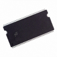
MT46V32M4TG-6T:D TR Micron Technology Inc, MT46V32M4TG-6T:D TR Datasheet - Page 69

MT46V32M4TG-6T:D TR
Manufacturer Part Number
MT46V32M4TG-6T:D TR
Description
IC DDR SDRAM 128MBIT 6NS 66TSOP
Manufacturer
Micron Technology Inc
Datasheet
1.MT46V32M4TG-6TD_TR.pdf
(93 pages)
Specifications of MT46V32M4TG-6T:D TR
Format - Memory
RAM
Memory Type
DDR SDRAM
Memory Size
128M (32Mx4)
Speed
6ns
Interface
Parallel
Voltage - Supply
2.3 V ~ 2.7 V
Operating Temperature
0°C ~ 70°C
Package / Case
66-TSOP
Lead Free Status / RoHS Status
Contains lead / RoHS non-compliant
Other names
557-1024-2
Notes
09005aef8074a655
128MBDDRx4x8x16_2.fm - Rev. J 4/05 EN
10. I
11. Enables on-chip refresh and address counters.
12. IDD specifications are tested after the device is properly initialized, and is averaged at
13. This parameter is sampled. V
14. For slew rates less than 1V/ns and greater than or equal to 0.5Vns. If slew rate is less
1. All voltages referenced to V
2. Tests for AC timing, I
3. Outputs (except for I
4. AC timing and IDD tests may use a V
5. The AC and DC input level specifications are as defined in the SSTL_2 Standard (i.e.,
6. V
7. V
8. V
9. The value of V
Output
(V
OUT
at nominal reference/supply voltage levels, but the related specifications and device
operation are guaranteed for the full voltage range specified.
ment, but input timing is still referenced to V
and parameter specifications are guaranteed for the specified AC input levels under
normal use conditions. The minimum slew rate for the input signals used to test the
device is 1V/ns in the range between V
the receiver will effectively switch as a result of the signal crossing the AC input level,
and will remain in that state as long as the signal does not ring back above [below] the
DC input LOW [HIGH] level).
the DC level of the same. Peak-to-peak noise (non-common mode) on V
exceed ±2 percent of the DC value. Thus, from V
error and an additional ±25mV for AC noise. This measurement is to be taken at the
nearest V
resistors, is expected to be set equal to V
of V
level on CK#.
must track variations in the DC level of the same.
with minimum cycle times at CL = 3 for -5B, CL = 2.5 for -6/-6T and -75, and CL=2 for
-75E/-75Z speeds with the outputs open.
the defined cycle rate.
T
pins, reflecting the fact that they are matched in loading.
than 0.5V/ns, timing must be derated:
reduction in slew rate from 500mV/ns, while
exceeds 4.5V/ns, functionality is uncertain. For -5B, -6, and -6T speed grades, slew
rates must be greater than or equal 0.5V/ns.
DD
REF
A
TT
ID
)
=25°C V
REF
is not applied directly to the device. V
is the magnitude of the difference between the input level on CK and the input
is dependent on output loading and cycle rates. Specified values are obtained
is expected to equal V
V
TT
.
50
30pF
Reference
Point
REF
OUT
by-pass capacitor.
(DC)=V
IX
and V
DD
DD
DD
MP
measurements) measured with equivalent load:
, and electrical AC and DC characteristics may be conducted
Q/2, V
are expected to equal V
DD
69
SS
.
DD
Q/2 of the transmitting device and to track variations in
OUT
=+2.5V±0.2V, V
(peak to peak)=0.2V. DM input is grouped with I/O
Micron Technology, Inc., reserves the right to change products or specifications without notice.
IL
IL
-to-V
t
IS has an additional 50ps per each 100mV/ns
(AC) and V
REF
TT
IH
128Mb: x4, x8, x16 DDR SDRAM
and must track variations in the DC level
REF
is a system supply for signal termination
swing of up to 1.5V in the test environ-
DD
t
IH has 0pF is unaffected. If slew rate
DD
(or to the crossing point for CK/CK#),
DD
Q=+2.5V±0.2V, V
Q/2, V
IH
Q/2 of the transmitting device and
(AC).
REF
©2000 Micron Technology, Inc. All rights reserved.
is allowed ±25mV for DC
REF
=V
SS
REF
, f=100MHz,
may not
Notes


