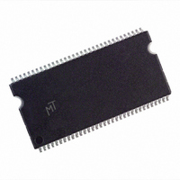
MT46V32M4TG-6T:D TR Micron Technology Inc, MT46V32M4TG-6T:D TR Datasheet - Page 35

MT46V32M4TG-6T:D TR
Manufacturer Part Number
MT46V32M4TG-6T:D TR
Description
IC DDR SDRAM 128MBIT 6NS 66TSOP
Manufacturer
Micron Technology Inc
Datasheet
1.MT46V32M4TG-6TD_TR.pdf
(93 pages)
Specifications of MT46V32M4TG-6T:D TR
Format - Memory
RAM
Memory Type
DDR SDRAM
Memory Size
128M (32Mx4)
Speed
6ns
Interface
Parallel
Voltage - Supply
2.3 V ~ 2.7 V
Operating Temperature
0°C ~ 70°C
Package / Case
66-TSOP
Lead Free Status / RoHS Status
Contains lead / RoHS non-compliant
Other names
557-1024-2
WRITEs
09005aef8074a655
128MBDDRx4x8x16_2.fm - Rev. J 4/05 EN
Note:
WRITE bursts are initiated with a WRITE command, as shown in Figure 20.
The starting column and bank addresses are provided with the WRITE command, and
auto precharge is either enabled or disabled for that access. If auto precharge is enabled,
the row being accessed is precharged at the completion of the burst and after the
time.
During WRITE bursts, the first valid data-in element will be registered on the first rising
edge of DQS following the WRITE command, and subsequent data elements will be reg-
istered on successive edges of DQS. The LOW state on DQS between the WRITE com-
mand and the first rising edge is known as the write preamble; the LOW state on DQS
following the last data-in element is known as the write postamble.
The time between the WRITE command and the first corresponding rising edge of
DQS (
cent of one clock cycle and 72
percent to 128 percent of one clock cycle for DDR400). All of the WRITE diagrams
show the nominal case, and where the two extreme cases (i.e.,
t
page 37 shows the nominal case and the extremes of
completion of a burst, assuming no other commands have been initiated, the DQ
will remain High-Z and any additional input data will be ignored.
Data for any WRITE burst may be concatenated with or truncated with a subsequent
WRITE command. In either case, a continuous flow of input data can be maintained.
The new WRITE command can be issued on any positive edge of clock following the pre-
vious WRITE command. The first data element from the new burst is applied after either
the last element of a completed burst or the last desired data element of a longer burst
which is being truncated. The new WRITE command should be issued x cycles after the
first WRITE command, where x equals the number of desired data element pairs (pairs
are required by the 2n-prefetch architecture).
Figure 22 on page 38 shows concatenated bursts of 4. An example of nonconsecutive
WRITEs is shown in Figure 23 on page 39. Full-speed random write accesses within a
page or pages can be performed as shown in Figure 24 on page 40.
DQSS [MAX]) might not be
For the WRITE commands used in the following illustrations, auto precharge is dis-
abled.
t
DQSS) is specified with a relatively wide range (from 75 percent to 125 per-
intuitive, they have also been included. Figure 21 on
35
Micron Technology, Inc., reserves the right to change products or specifications without notice.
128Mb: x4, x8, x16 DDR SDRAM
t
DQSS for a burst of 4. Upon
©2000 Micron Technology, Inc. All rights reserved.
t
DQSS [MIN] an
Operations
t
WR
d


