HD6417750RF240DV Renesas Electronics America, HD6417750RF240DV Datasheet - Page 76
HD6417750RF240DV
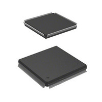
Manufacturer Part Number
HD6417750RF240DV
Description
MPU 3V 16K I-TEMP,PB-FREE 208-QF
Manufacturer
Renesas Electronics America
Series
SuperH® SH7750r
Datasheet
1.D6417750RBP240DV.pdf
(1164 pages)
Specifications of HD6417750RF240DV
Core Processor
SH-4
Core Size
32-Bit
Speed
240MHz
Connectivity
EBI/EMI, FIFO, SCI, SmartCard
Peripherals
DMA, POR, WDT
Number Of I /o
28
Program Memory Type
ROMless
Ram Size
48K x 8
Voltage - Supply (vcc/vdd)
1.4 V ~ 1.6 V
Oscillator Type
External
Operating Temperature
-40°C ~ 85°C
Package / Case
208-QFP
Lead Free Status / RoHS Status
Lead free / RoHS Compliant
Eeprom Size
-
Program Memory Size
-
Data Converters
-
Available stocks
Company
Part Number
Manufacturer
Quantity
Price
Company:

Part Number:
HD6417750RF240DV
Manufacturer:
HITACHI
Quantity:
7 287


Figure 22.18 SRAM Bus Cycle: Basic Bus Cycle (No Wait, Address Setup/Hold Time
Figure 22.19 Burst ROM Bus Cycle (No Wait) .......................................................................... 960
Figure 22.20 Burst ROM Bus Cycle (1st Data: One Internal Wait + One External Wait;
Figure 22.21 Burst ROM Bus Cycle (No Wait, Address Setup/Hold Time Insertion, AnS = 1,
Figure 22.22 Burst ROM Bus Cycle (One Internal Wait + One External Wait) ......................... 963
Figure 22.23 Synchronous DRAM Auto-Precharge Read Bus Cycle: Single (RCD[1:0] = 01,
Figure 22.24 Synchronous DRAM Auto-Precharge Read Bus Cycle: Burst (RCD[1:0] = 01,
Figure 22.25 Synchronous DRAM Normal Read Bus Cycle: ACT + READ Commands,
Figure 22.26 Synchronous DRAM Normal Read Bus Cycle: PRE + ACT + READ Commands,
Figure 22.27 Synchronous DRAM Normal Read Bus Cycle: READ Command, Burst
Figure 22.28 Synchronous DRAM Auto-Precharge Write Bus Cycle: Single (RCD[1:0] = 01,
Figure 22.29 Synchronous DRAM Auto-Precharge Write Bus Cycle: Burst (RCD[1:0] = 01,
Figure 22.30 Synchronous DRAM Normal Write Bus Cycle: ACT + WRITE Commands,
Figure 22.31 Synchronous DRAM Normal Write Bus Cycle: PRE + ACT + WRITE Commands,
Figure 22.32 Synchronous DRAM Normal Write Bus Cycle: WRITE Command, Burst
Figure 22.33 Synchronous DRAM Bus Cycle: Synchronous DRAM Precharge Command
Figure 22.34 Synchronous DRAM Bus Cycle: Synchronous DRAM Auto-Refresh
Figure 22.35 Synchronous DRAM Bus Cycle: Synchronous DRAM Self-Refresh
Figure 22.36 (a) Synchronous DRAM Bus Cycle: Synchronous DRAM Mode Register
Figure 22.36 (b) Synchronous DRAM Bus Cycle: Synchronous DRAM Mode Register
Figure 22.37 DRAM Bus Cycles (1) RCD[1:0] = 00, AnW[2:0] = 000, TPC[2:0] = 001
Rev.7.00 Oct. 10, 2008 Page lxxiv of lxxxiv
REJ09B0366-0700
Insertion, AnS = 1, AnH = 1) ................................................................................. 959
2nd/3rd/4th Data: One Internal Wait)..................................................................... 961
AnH = 1) ................................................................................................................ 962
CAS Latency = 3, TPC[2:0] = 011) ....................................................................... 964
CAS Latency = 3, TPC[2:0] = 011) ....................................................................... 965
Burst (RASD = 1, RCD[1:0] = 01, CAS Latency = 3)........................................... 966
Burst ((RASD = 1, RCD[1:0] = 01, TPC[2:0] = 001, CAS Latency = 3) .............. 967
((RASD = 1, CAS Latency = 3) ............................................................................. 968
TPC[2:0] = 001, TRWL[2:0] = 010) ...................................................................... 969
TPC[2:0] = 001, TRWL[2:0] = 010) ...................................................................... 970
Burst (RASD = 1, RCD[1:0] = 01, TRWL[2:0] = 010) ......................................... 971
Burst (RASD = 1, RCD[1:0] = 01, TPC[2:0] = 001, TRWL[2:0] = 010) .............. 972
(RASD = 1, TRWL[2:0] = 010) ............................................................................. 973
(RASD = 1, TPC[2:0] = 001) ................................................................................. 974
(TRAS = 1, TRC[2:0] = 001) ................................................................................. 975
(TRC[2:0] = 001) ................................................................................................... 976
Setting (PALL)....................................................................................................... 977
Setting (SET).......................................................................................................... 978
(2) RCD[1:0] = 01, AnW[2:0] = 001, TPC[2:0] = 010 .......................................... 979
Related parts for HD6417750RF240DV
Image
Part Number
Description
Manufacturer
Datasheet
Request
R

Part Number:
Description:
KIT STARTER FOR M16C/29
Manufacturer:
Renesas Electronics America
Datasheet:

Part Number:
Description:
KIT STARTER FOR R8C/2D
Manufacturer:
Renesas Electronics America
Datasheet:

Part Number:
Description:
R0K33062P STARTER KIT
Manufacturer:
Renesas Electronics America
Datasheet:

Part Number:
Description:
KIT STARTER FOR R8C/23 E8A
Manufacturer:
Renesas Electronics America
Datasheet:

Part Number:
Description:
KIT STARTER FOR R8C/25
Manufacturer:
Renesas Electronics America
Datasheet:

Part Number:
Description:
KIT STARTER H8S2456 SHARPE DSPLY
Manufacturer:
Renesas Electronics America
Datasheet:

Part Number:
Description:
KIT STARTER FOR R8C38C
Manufacturer:
Renesas Electronics America
Datasheet:

Part Number:
Description:
KIT STARTER FOR R8C35C
Manufacturer:
Renesas Electronics America
Datasheet:

Part Number:
Description:
KIT STARTER FOR R8CL3AC+LCD APPS
Manufacturer:
Renesas Electronics America
Datasheet:
Part Number:
Description:
KIT STARTER FOR RX610
Manufacturer:
Renesas Electronics America
Datasheet:

Part Number:
Description:
KIT STARTER FOR R32C/118
Manufacturer:
Renesas Electronics America
Datasheet:

Part Number:
Description:
KIT DEV RSK-R8C/26-29
Manufacturer:
Renesas Electronics America
Datasheet:

Part Number:
Description:
KIT STARTER FOR SH7124
Manufacturer:
Renesas Electronics America
Datasheet:

Part Number:
Description:
KIT STARTER FOR H8SX/1622
Manufacturer:
Renesas Electronics America
Datasheet:

Part Number:
Description:
KIT DEV FOR SH7203
Manufacturer:
Renesas Electronics America
Datasheet: