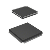
HD6417750RF240DV Renesas Electronics America, HD6417750RF240DV Datasheet - Page 67

HD6417750RF240DV
Manufacturer Part Number
HD6417750RF240DV
Description
MPU 3V 16K I-TEMP,PB-FREE 208-QF
Manufacturer
Renesas Electronics America
Series
SuperH® SH7750r
Datasheet
1.D6417750RBP240DV.pdf
(1164 pages)
Specifications of HD6417750RF240DV
Core Processor
SH-4
Core Size
32-Bit
Speed
240MHz
Connectivity
EBI/EMI, FIFO, SCI, SmartCard
Peripherals
DMA, POR, WDT
Number Of I /o
28
Program Memory Type
ROMless
Ram Size
48K x 8
Voltage - Supply (vcc/vdd)
1.4 V ~ 1.6 V
Oscillator Type
External
Operating Temperature
-40°C ~ 85°C
Package / Case
208-QFP
Lead Free Status / RoHS Status
Lead free / RoHS Compliant
Eeprom Size
-
Program Memory Size
-
Data Converters
-
Available stocks
Company
Part Number
Manufacturer
Quantity
Price
Company:
Part Number:
HD6417750RF240DV
Manufacturer:
HITACHI
Quantity:
7 287
- Current page: 67 of 1164
- Download datasheet (7Mb)
Figure 9.8
Figure 9.9
Figure 9.10 STATUS Output in Deep Sleep → Power-On Reset Sequence ............................. 281
Figure 9.11 STATUS Output in Deep Sleep → Manual Reset Sequence ................................. 282
Figure 9.12 Hardware Standby Mode Timing (When CA = Low in Normal Operation) .......... 283
Figure 9.13 Hardware Standby Mode Timing (When CA = Low in WDT Operation) ............. 284
Figure 9.14 Timing When Power Other than VDD-RTC Is Off................................................ 285
Figure 9.15 Timing When VDD-RTC Power Is Off → On....................................................... 285
Section 10 Clock Oscillation Circuits
Figure 10.1 (1) Block Diagram of CPG (SH7750, SH7750S) ................................................... 289
Figure 10.1 (2) Block Diagram of CPG (SH7750R).................................................................. 290
Figure 10.2 Block Diagram of WDT ......................................................................................... 300
Figure 10.3 Writing to WTCNT and WTCSR........................................................................... 305
Figure 10.4 Points for Attention when Using Crystal Resonator............................................... 307
Figure 10.5 Points for Attention when Using PLL Oscillator Circuit ....................................... 308
Section 11 Realtime Clock (RTC)
Figure 11.1 Block Diagram of RTC .......................................................................................... 312
Figure 11.2 Examples of Time Setting Procedures.................................................................... 329
Figure 11.3 Examples of Time Reading Procedures.................................................................. 331
Figure 11.4 Example of Use of Alarm Function........................................................................ 332
Figure 11.5 Example of Crystal Oscillator Circuit Connection................................................. 334
Section 12 Timer Unit (TMU)
Figure 12.1 Block Diagram of TMU ......................................................................................... 338
Figure 12.2 Example of Count Operation Setting Procedure .................................................... 351
Figure 12.3 TCNT Auto-Reload Operation ............................................................................... 352
Figure 12.4 Count Timing when Operating on Internal Clock .................................................. 352
Figure 12.5 Count Timing when Operating on External Clock ................................................. 353
Figure 12.6 Count Timing when Operating on On-Chip RTC Output Clock............................ 353
Figure 12.7 Operation Timing when Using Input Capture Function ......................................... 354
Section 13 Bus State Controller (BSC)
Figure 13.1 Block Diagram of BSC........................................................................................... 359
Figure 13.2 Correspondence between Virtual Address Space and External Memory Space..... 365
Figure 13.3 External Memory Space Allocation ....................................................................... 367
Figure 13.4 Example of RDY Sampling Timing at which BCR4 Is Set
Figure 13.5 Writing to RTCSR, RTCNT, RTCOR, and RFCR................................................. 421
STATUS Output in Sleep → Manual Reset Sequence........................................... 280
STATUS Output in Deep Sleep → Interrupt Sequence ......................................... 281
(Two Wait Cycles Are Inserted by WCR2)............................................................ 385
Rev.7.00 Oct. 10, 2008 Page lxv of lxxxiv
REJ09B0366-0700
Related parts for HD6417750RF240DV
Image
Part Number
Description
Manufacturer
Datasheet
Request
R

Part Number:
Description:
KIT STARTER FOR M16C/29
Manufacturer:
Renesas Electronics America
Datasheet:

Part Number:
Description:
KIT STARTER FOR R8C/2D
Manufacturer:
Renesas Electronics America
Datasheet:

Part Number:
Description:
R0K33062P STARTER KIT
Manufacturer:
Renesas Electronics America
Datasheet:

Part Number:
Description:
KIT STARTER FOR R8C/23 E8A
Manufacturer:
Renesas Electronics America
Datasheet:

Part Number:
Description:
KIT STARTER FOR R8C/25
Manufacturer:
Renesas Electronics America
Datasheet:

Part Number:
Description:
KIT STARTER H8S2456 SHARPE DSPLY
Manufacturer:
Renesas Electronics America
Datasheet:

Part Number:
Description:
KIT STARTER FOR R8C38C
Manufacturer:
Renesas Electronics America
Datasheet:

Part Number:
Description:
KIT STARTER FOR R8C35C
Manufacturer:
Renesas Electronics America
Datasheet:

Part Number:
Description:
KIT STARTER FOR R8CL3AC+LCD APPS
Manufacturer:
Renesas Electronics America
Datasheet:

Part Number:
Description:
KIT STARTER FOR RX610
Manufacturer:
Renesas Electronics America
Datasheet:

Part Number:
Description:
KIT STARTER FOR R32C/118
Manufacturer:
Renesas Electronics America
Datasheet:

Part Number:
Description:
KIT DEV RSK-R8C/26-29
Manufacturer:
Renesas Electronics America
Datasheet:

Part Number:
Description:
KIT STARTER FOR SH7124
Manufacturer:
Renesas Electronics America
Datasheet:

Part Number:
Description:
KIT STARTER FOR H8SX/1622
Manufacturer:
Renesas Electronics America
Datasheet:

Part Number:
Description:
KIT DEV FOR SH7203
Manufacturer:
Renesas Electronics America
Datasheet:


