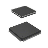
HD6417750RF240DV Renesas Electronics America, HD6417750RF240DV Datasheet - Page 692

HD6417750RF240DV
Manufacturer Part Number
HD6417750RF240DV
Description
MPU 3V 16K I-TEMP,PB-FREE 208-QF
Manufacturer
Renesas Electronics America
Series
SuperH® SH7750r
Datasheet
1.D6417750RBP240DV.pdf
(1164 pages)
Specifications of HD6417750RF240DV
Core Processor
SH-4
Core Size
32-Bit
Speed
240MHz
Connectivity
EBI/EMI, FIFO, SCI, SmartCard
Peripherals
DMA, POR, WDT
Number Of I /o
28
Program Memory Type
ROMless
Ram Size
48K x 8
Voltage - Supply (vcc/vdd)
1.4 V ~ 1.6 V
Oscillator Type
External
Operating Temperature
-40°C ~ 85°C
Package / Case
208-QFP
Lead Free Status / RoHS Status
Lead free / RoHS Compliant
Eeprom Size
-
Program Memory Size
-
Data Converters
-
Available stocks
Company
Part Number
Manufacturer
Quantity
Price
Company:
Part Number:
HD6417750RF240DV
Manufacturer:
HITACHI
Quantity:
7 287
- Current page: 692 of 1164
- Download datasheet (7Mb)
Section 14 Direct Memory Access Controller (DMAC)
• TDACK: Reply strobe signal for external device from DMAC
• ID1, ID0: Channel number notification signals
Data Transfer Request Format
The data transfer request format (DTR format) consists of 64 bits, with connection to D[63:0]. In
the case of normal data transfer mode (channel 0, except channel 0) and the handshake protocol
using the data bus, the transfer data size, read/write access, channel number, transfer request
mode, number of transfers, and transfer source or transfer destination address are specified. A
specification in bits 47–32 is invalid.
In the SH7750, only single address mode can be set in normal data transfer mode (channel 0).
With the DTR format, DS = (0: MD = 10, 11, 1: MD = 01), RL = 0, AL = 0, DM[1:0] = 01,
SM[1:0] = 01, RS[3:0] = (0010: R/W = 0, 0011: R/W = 1), TM = (0: MD = 11, 1: MD = 01, 10),
TS[2:0] = (SZ), and IE = 0 settings are made in DMA channel control register 0, COUNT is set in
transfer count register 0, and ADDRESS is set in source/destination address register 0. Therefore,
in DDT mode, the above control registers cannot be written to by the CPU, but can be read.
In the SH7750S, DMAC control registers CHCR0, SAR0, DAR0, and DMATCR0 can be written
to and read by the CPU even in normal data transfer mode (channel 0). Caution is necessary in this
case, as a DMAC control register written to by the CPU will be overwritten by a subsequent
transfer request (MD[1:0] = 01, 10, or 11) using the DTR format.
Rev.7.00 Oct. 10, 2008 Page 606 of 1074
REJ09B0366-0700
63 61 60 59
SZ
⎯ In the case of direct data transfer mode (valid only for channel 2), a direct transfer request
The assert timing of this signal is the same as the DACKn assert timing of the memory
interfaces.
Note that it is a low active signal.
⎯ 00: Channel 0 (means demand data transfer)
⎯ 01: Channel 1
⎯ 10: Channel 2
⎯ 11: Channel 3
can be made to channel 2 by asserting DBREQ and TR simultaneously.
R/W
ID
57
MD
Figure 14.25 Data Transfer Request Format
55
COUNT
48
(Reserved)
31
ADDRESS
0
Related parts for HD6417750RF240DV
Image
Part Number
Description
Manufacturer
Datasheet
Request
R

Part Number:
Description:
KIT STARTER FOR M16C/29
Manufacturer:
Renesas Electronics America
Datasheet:

Part Number:
Description:
KIT STARTER FOR R8C/2D
Manufacturer:
Renesas Electronics America
Datasheet:

Part Number:
Description:
R0K33062P STARTER KIT
Manufacturer:
Renesas Electronics America
Datasheet:

Part Number:
Description:
KIT STARTER FOR R8C/23 E8A
Manufacturer:
Renesas Electronics America
Datasheet:

Part Number:
Description:
KIT STARTER FOR R8C/25
Manufacturer:
Renesas Electronics America
Datasheet:

Part Number:
Description:
KIT STARTER H8S2456 SHARPE DSPLY
Manufacturer:
Renesas Electronics America
Datasheet:

Part Number:
Description:
KIT STARTER FOR R8C38C
Manufacturer:
Renesas Electronics America
Datasheet:

Part Number:
Description:
KIT STARTER FOR R8C35C
Manufacturer:
Renesas Electronics America
Datasheet:

Part Number:
Description:
KIT STARTER FOR R8CL3AC+LCD APPS
Manufacturer:
Renesas Electronics America
Datasheet:

Part Number:
Description:
KIT STARTER FOR RX610
Manufacturer:
Renesas Electronics America
Datasheet:

Part Number:
Description:
KIT STARTER FOR R32C/118
Manufacturer:
Renesas Electronics America
Datasheet:

Part Number:
Description:
KIT DEV RSK-R8C/26-29
Manufacturer:
Renesas Electronics America
Datasheet:

Part Number:
Description:
KIT STARTER FOR SH7124
Manufacturer:
Renesas Electronics America
Datasheet:

Part Number:
Description:
KIT STARTER FOR H8SX/1622
Manufacturer:
Renesas Electronics America
Datasheet:

Part Number:
Description:
KIT DEV FOR SH7203
Manufacturer:
Renesas Electronics America
Datasheet:


