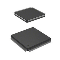
HD6417750RF240DV Renesas Electronics America, HD6417750RF240DV Datasheet - Page 237

HD6417750RF240DV
Manufacturer Part Number
HD6417750RF240DV
Description
MPU 3V 16K I-TEMP,PB-FREE 208-QF
Manufacturer
Renesas Electronics America
Series
SuperH® SH7750r
Datasheet
1.D6417750RBP240DV.pdf
(1164 pages)
Specifications of HD6417750RF240DV
Core Processor
SH-4
Core Size
32-Bit
Speed
240MHz
Connectivity
EBI/EMI, FIFO, SCI, SmartCard
Peripherals
DMA, POR, WDT
Number Of I /o
28
Program Memory Type
ROMless
Ram Size
48K x 8
Voltage - Supply (vcc/vdd)
1.4 V ~ 1.6 V
Oscillator Type
External
Operating Temperature
-40°C ~ 85°C
Package / Case
208-QFP
Lead Free Status / RoHS Status
Lead free / RoHS Compliant
Eeprom Size
-
Program Memory Size
-
Data Converters
-
Available stocks
Company
Part Number
Manufacturer
Quantity
Price
Company:
Part Number:
HD6417750RF240DV
Manufacturer:
HITACHI
Quantity:
7 287
- Current page: 237 of 1164
- Download datasheet (7Mb)
5.3
5.3.1
In exception handling, the contents of the program counter (PC), status register (SR), and R15 are
saved in the saved program counter (SPC), saved status register (SSR), and saved general
register15(SGR), and the CPU starts execution of the appropriate exception handling routine
according to the vector address. An exception handling routine is a program written by the user to
handle a specific exception. The exception handling routine is terminated and control returned to
the original program by executing a return-from-exception instruction (RTE). This instruction
restores the PC and SR contents and returns control to the normal processing routine at the point at
which the exception occurred.
The SGR contents are not written back to R15 by an RTE instruction.
The basic processing flow is as follows. See section 2, Programming Model, for the meaning of
the individual SR bits.
1. The PC, SR, and R15 contents are saved in SPC, SSR, and SGR.
2. The block bit (BL) in SR is set to 1.
3. The mode bit (MD) in SR is set to 1.
4. The register bank bit (RB) in SR is set to 1.
5. In a reset, the FPU disable bit (FD) in SR is cleared to 0.
6. The exception code is written to bits 11–0 of the exception event register (EXPEVT) or
7. The CPU branches to the determined exception handling vector address, and the exception
5.3.2
The reset vector address is fixed at H'A000 0000. General exception and interrupt vector addresses
are determined by adding the offset for the specific event to the vector base address, which is set
by software in the vector base register (VBR). In the case of the TLB miss exception, for example,
the offset is H'0000 0400, so if H'9C08 0000 is set in VBR, the exception handling vector address
will be H'9C08 0400. If a further exception occurs at the exception handling vector address, a
duplicate exception will result, and recovery will be difficult; therefore, fixed physical addresses
(P1, P2) should be specified for vector addresses.
interrupt event register (INTEVT).
handling routine begins.
Exception Handling Functions
Exception Handling Flow
Exception Handling Vector Addresses
Rev.7.00 Oct. 10, 2008 Page 151 of 1074
Section 5 Exceptions
REJ09B0366-0700
Related parts for HD6417750RF240DV
Image
Part Number
Description
Manufacturer
Datasheet
Request
R

Part Number:
Description:
KIT STARTER FOR M16C/29
Manufacturer:
Renesas Electronics America
Datasheet:

Part Number:
Description:
KIT STARTER FOR R8C/2D
Manufacturer:
Renesas Electronics America
Datasheet:

Part Number:
Description:
R0K33062P STARTER KIT
Manufacturer:
Renesas Electronics America
Datasheet:

Part Number:
Description:
KIT STARTER FOR R8C/23 E8A
Manufacturer:
Renesas Electronics America
Datasheet:

Part Number:
Description:
KIT STARTER FOR R8C/25
Manufacturer:
Renesas Electronics America
Datasheet:

Part Number:
Description:
KIT STARTER H8S2456 SHARPE DSPLY
Manufacturer:
Renesas Electronics America
Datasheet:

Part Number:
Description:
KIT STARTER FOR R8C38C
Manufacturer:
Renesas Electronics America
Datasheet:

Part Number:
Description:
KIT STARTER FOR R8C35C
Manufacturer:
Renesas Electronics America
Datasheet:

Part Number:
Description:
KIT STARTER FOR R8CL3AC+LCD APPS
Manufacturer:
Renesas Electronics America
Datasheet:

Part Number:
Description:
KIT STARTER FOR RX610
Manufacturer:
Renesas Electronics America
Datasheet:

Part Number:
Description:
KIT STARTER FOR R32C/118
Manufacturer:
Renesas Electronics America
Datasheet:

Part Number:
Description:
KIT DEV RSK-R8C/26-29
Manufacturer:
Renesas Electronics America
Datasheet:

Part Number:
Description:
KIT STARTER FOR SH7124
Manufacturer:
Renesas Electronics America
Datasheet:

Part Number:
Description:
KIT STARTER FOR H8SX/1622
Manufacturer:
Renesas Electronics America
Datasheet:

Part Number:
Description:
KIT DEV FOR SH7203
Manufacturer:
Renesas Electronics America
Datasheet:


