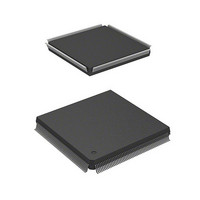
HD6417750RF240DV Renesas Electronics America, HD6417750RF240DV Datasheet - Page 151

HD6417750RF240DV
Manufacturer Part Number
HD6417750RF240DV
Description
MPU 3V 16K I-TEMP,PB-FREE 208-QF
Manufacturer
Renesas Electronics America
Series
SuperH® SH7750r
Datasheet
1.D6417750RBP240DV.pdf
(1164 pages)
Specifications of HD6417750RF240DV
Core Processor
SH-4
Core Size
32-Bit
Speed
240MHz
Connectivity
EBI/EMI, FIFO, SCI, SmartCard
Peripherals
DMA, POR, WDT
Number Of I /o
28
Program Memory Type
ROMless
Ram Size
48K x 8
Voltage - Supply (vcc/vdd)
1.4 V ~ 1.6 V
Oscillator Type
External
Operating Temperature
-40°C ~ 85°C
Package / Case
208-QFP
Lead Free Status / RoHS Status
Lead free / RoHS Compliant
Eeprom Size
-
Program Memory Size
-
Data Converters
-
Available stocks
Company
Part Number
Manufacturer
Quantity
Price
Company:
Part Number:
HD6417750RF240DV
Manufacturer:
HITACHI
Quantity:
7 287
- Current page: 151 of 1164
- Download datasheet (7Mb)
• RM: Rounding mode
• Bits 22 to 31: Reserved
Floating-point communication register, FPUL (32 bits, initial value undefined): Data transfer
between FPU registers and CPU registers is carried out via the FPUL register.
Programming Note: When SZ = 1 and big endian mode is selected, FMOV can be used for
double-precision floating-point load or store operations. In little endian mode, two 32-bit data size
moves must be executed, with SZ = 0, to load or store a double-precision floating-point number.
2.3
Appendix A, Address List shows the control registers mapped to memory. The control registers
are double-mapped to the following two memory areas. All registers have two addresses.
H'1C00 0000–H'1FFF FFFF
H'FC00 0000–H'FFFF FFFF
These two areas are used as follows.
• H'1C00 0000–H'1FFF FFFF
• H'FC00 0000–H'FFFF FFFF
When an FPU operation instruction is executed, the FPU exception cause field is cleared to
zero first. When the next FPU exception is occured, the corresponding bits in the FPU
exception cause field and FPU exception flag field are set to 1. The FPU exception flag field
holds the status of the exception generated after the field was last cleared.
RM = 00: Round to Nearest
RM = 01: Round to Zero
RM = 10: Reserved
RM = 11: Reserved
This area must be accessed using the address translation function of the MMU. Setting the
page number of this area to the corresponding filed of the TLB enables access to a memory-
mapped register. Accessing this area without using the address translation function of the
MMU is not guaranteed.
Access to area H'FF00 0000–H'FFFF FFFF in user mode will cause an address error. Memory-
mapped registers can be referenced in user mode by means of access that involves address
translation.
Memory-Mapped Registers
Rev.7.00 Oct. 10, 2008 Page 65 of 1074
Section 2 Programming Model
REJ09B0366-0700
Related parts for HD6417750RF240DV
Image
Part Number
Description
Manufacturer
Datasheet
Request
R

Part Number:
Description:
KIT STARTER FOR M16C/29
Manufacturer:
Renesas Electronics America
Datasheet:

Part Number:
Description:
KIT STARTER FOR R8C/2D
Manufacturer:
Renesas Electronics America
Datasheet:

Part Number:
Description:
R0K33062P STARTER KIT
Manufacturer:
Renesas Electronics America
Datasheet:

Part Number:
Description:
KIT STARTER FOR R8C/23 E8A
Manufacturer:
Renesas Electronics America
Datasheet:

Part Number:
Description:
KIT STARTER FOR R8C/25
Manufacturer:
Renesas Electronics America
Datasheet:

Part Number:
Description:
KIT STARTER H8S2456 SHARPE DSPLY
Manufacturer:
Renesas Electronics America
Datasheet:

Part Number:
Description:
KIT STARTER FOR R8C38C
Manufacturer:
Renesas Electronics America
Datasheet:

Part Number:
Description:
KIT STARTER FOR R8C35C
Manufacturer:
Renesas Electronics America
Datasheet:

Part Number:
Description:
KIT STARTER FOR R8CL3AC+LCD APPS
Manufacturer:
Renesas Electronics America
Datasheet:

Part Number:
Description:
KIT STARTER FOR RX610
Manufacturer:
Renesas Electronics America
Datasheet:

Part Number:
Description:
KIT STARTER FOR R32C/118
Manufacturer:
Renesas Electronics America
Datasheet:

Part Number:
Description:
KIT DEV RSK-R8C/26-29
Manufacturer:
Renesas Electronics America
Datasheet:

Part Number:
Description:
KIT STARTER FOR SH7124
Manufacturer:
Renesas Electronics America
Datasheet:

Part Number:
Description:
KIT STARTER FOR H8SX/1622
Manufacturer:
Renesas Electronics America
Datasheet:

Part Number:
Description:
KIT DEV FOR SH7203
Manufacturer:
Renesas Electronics America
Datasheet:


