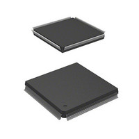
HD6417750RF240DV Renesas Electronics America, HD6417750RF240DV Datasheet - Page 71

HD6417750RF240DV
Manufacturer Part Number
HD6417750RF240DV
Description
MPU 3V 16K I-TEMP,PB-FREE 208-QF
Manufacturer
Renesas Electronics America
Series
SuperH® SH7750r
Datasheet
1.D6417750RBP240DV.pdf
(1164 pages)
Specifications of HD6417750RF240DV
Core Processor
SH-4
Core Size
32-Bit
Speed
240MHz
Connectivity
EBI/EMI, FIFO, SCI, SmartCard
Peripherals
DMA, POR, WDT
Number Of I /o
28
Program Memory Type
ROMless
Ram Size
48K x 8
Voltage - Supply (vcc/vdd)
1.4 V ~ 1.6 V
Oscillator Type
External
Operating Temperature
-40°C ~ 85°C
Package / Case
208-QFP
Lead Free Status / RoHS Status
Lead free / RoHS Compliant
Eeprom Size
-
Program Memory Size
-
Data Converters
-
Available stocks
Company
Part Number
Manufacturer
Quantity
Price
Company:
Part Number:
HD6417750RF240DV
Manufacturer:
HITACHI
Quantity:
7 287
- Current page: 71 of 1164
- Download datasheet (7Mb)
Figure 14.14 Dual Address Mode/Burst Mode External Bus → External Bus/DREQ
Figure 14.15 Dual Address Mode/Burst Mode External Bus → External Bus/DREQ
Figure 14.16 Dual Address Mode/Cycle Steal Mode On-Chip SCI (Level Detection) →
Figure 14.17 Dual Address Mode/Cycle Steal Mode External Bus → On-Chip SCI
Figure 14.18 Single Address Mode/Cycle Steal Mode External Bus → External Bus/DREQ
Figure 14.19 Single Address Mode/Cycle Steal Mode External Bus → External Bus/DREQ
Figure 14.20 Single Address Mode/Burst Mode External Bus → External Bus/DREQ
Figure 14.21 Single Address Mode/Burst Mode External Bus → External Bus/DREQ
Figure 14.22 Single Address Mode/Burst Mode External Bus → External Bus/DREQ
Figure 14.23 On-Demand Transfer Mode Block Diagram .......................................................... 603
Figure 14.24 System Configuration in On-Demand Data Transfer Mode................................... 605
Figure 14.25 Data Transfer Request Format................................................................................ 606
Figure 14.26 Single Address Mode: Synchronous DRAM → External Device Longword Transfer
Figure 14.27 Single Address Mode: External Device → Synchronous DRAM Longword Transfer
Figure 14.28 Dual Address Mode/Synchronous DRAM → SRAM Longword Transfer ............ 611
Figure 14.29 Single Address Mode/Burst Mode/External Bus → External Device 32-Byte
Figure 14.30 Single Address Mode/Burst Mode/External Device → External Bus 32-Byte
Figure 14.31 Single Address Mode/Burst Mode/External Bus → External Device 32-Bit
Figure 14.32 Single Address Mode/Burst Mode/External Device → External Bus 32-Bit
Figure 14.33 Handshake Protocol Using Data Bus (Channel 0 On-Demand Data Transfer) ..... 616
Figure 14.34 Handshake Protocol without Use of Data Bus (Channel 0 On-Demand Data
(Level Detection), DACK (Read Cycle) ................................................................ 590
(Edge Detection), DACK (Read Cycle) ................................................................. 591
External Bus ........................................................................................................... 592
(Level Detection).................................................................................................... 593
(Level Detection).................................................................................................... 594
(Edge Detection) .................................................................................................... 595
(Level Detection).................................................................................................... 596
(Edge Detection) .................................................................................................... 597
(Level Detection)/32-Byte Block Transfer (Bus Width: 64 Bits, SDRAM:
Row Hit Write)....................................................................................................... 598
SDRAM auto-precharge Read bus cycle, burst (RCD[1:0] = 01, CAS latency = 3,
TPC[2:0] = 001)....................................................................................................... 609
SDRAM auto-precharge Write bus cycle, burst (RCD[1:0] = 01, TRWL[2:0] = 101,
TPC[2:0] = 001)....................................................................................................... 610
Block Transfer/Channel 0 On-Demand Data Transfer ........................................... 612
Block Transfer/Channel 0 On-Demand Data Transfer ........................................... 613
Transfer/Channel 0 On-Demand Data Transfer ..................................................... 614
Transfer/Channel 0 On-Demand Data Transfer ..................................................... 615
Transfer) ................................................................................................................. 617
Rev.7.00 Oct. 10, 2008 Page lxix of lxxxiv
REJ09B0366-0700
Related parts for HD6417750RF240DV
Image
Part Number
Description
Manufacturer
Datasheet
Request
R

Part Number:
Description:
KIT STARTER FOR M16C/29
Manufacturer:
Renesas Electronics America
Datasheet:

Part Number:
Description:
KIT STARTER FOR R8C/2D
Manufacturer:
Renesas Electronics America
Datasheet:

Part Number:
Description:
R0K33062P STARTER KIT
Manufacturer:
Renesas Electronics America
Datasheet:

Part Number:
Description:
KIT STARTER FOR R8C/23 E8A
Manufacturer:
Renesas Electronics America
Datasheet:

Part Number:
Description:
KIT STARTER FOR R8C/25
Manufacturer:
Renesas Electronics America
Datasheet:

Part Number:
Description:
KIT STARTER H8S2456 SHARPE DSPLY
Manufacturer:
Renesas Electronics America
Datasheet:

Part Number:
Description:
KIT STARTER FOR R8C38C
Manufacturer:
Renesas Electronics America
Datasheet:

Part Number:
Description:
KIT STARTER FOR R8C35C
Manufacturer:
Renesas Electronics America
Datasheet:

Part Number:
Description:
KIT STARTER FOR R8CL3AC+LCD APPS
Manufacturer:
Renesas Electronics America
Datasheet:

Part Number:
Description:
KIT STARTER FOR RX610
Manufacturer:
Renesas Electronics America
Datasheet:

Part Number:
Description:
KIT STARTER FOR R32C/118
Manufacturer:
Renesas Electronics America
Datasheet:

Part Number:
Description:
KIT DEV RSK-R8C/26-29
Manufacturer:
Renesas Electronics America
Datasheet:

Part Number:
Description:
KIT STARTER FOR SH7124
Manufacturer:
Renesas Electronics America
Datasheet:

Part Number:
Description:
KIT STARTER FOR H8SX/1622
Manufacturer:
Renesas Electronics America
Datasheet:

Part Number:
Description:
KIT DEV FOR SH7203
Manufacturer:
Renesas Electronics America
Datasheet:


