ATEVK1105 Atmel, ATEVK1105 Datasheet - Page 756
ATEVK1105
Manufacturer Part Number
ATEVK1105
Description
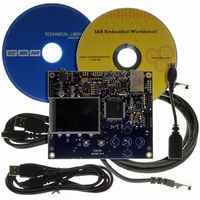
KIT EVAL FOR AT32UC3A0
Manufacturer
Atmel
Series
AVR®32r
Type
MCUr
Datasheets
1.ATAVRONE-PROBECBL.pdf
(16 pages)
2.ATEVK1104.pdf
(826 pages)
3.ATEVK1105.pdf
(28 pages)
Specifications of ATEVK1105
Contents
Evaluation Board, Software and Documentation
Processor To Be Evaluated
AT32UC3A0512
Processor Series
AVR
Data Bus Width
32 bit
Interface Type
USART, TWI, USB, SPI, Ethernet
Operating Supply Voltage
3.3 V
Silicon Manufacturer
Atmel
Core Architecture
AVR
Core Sub-architecture
AVR UC3
Silicon Core Number
AT32UC3A0512
Silicon Family Name
AVR
Kit Contents
Board CD Docs
Rohs Compliant
Yes
For Use With/related Products
AT32UC3A0
Lead Free Status / RoHS Status
Lead free / RoHS Compliant


36.9.7
32058J–AVR32–04/11
CANCEL_ACCESS
For write operations, 32 data bits must be provided, or the result will be undefined. For read
operations, shifting may be terminated once the required number of bits have been acquired.
Table 36-10. MEMORY_BLOCK_ACCESS details
The overhead using block word access is 4 cycles per 32 bits of data, resulting in an 88% trans-
fer efficiency, or 2.1 MBytes per second with a 20 MHz TCK frequency.
If a very slow memory location is accessed during a SAB memory access, it could take a very
long time until the busy bit is cleared, and the SAB becomes ready for the next operation. The
CANCEL_ACCESS instruction provides a possibility to abort an ongoing transfer and report a
timeout to the user.
When the CANCEL_ACCESS instruction is selected, the current access will be terminated as
soon as possible. There are no guarantees about how long this will take, as the hardware may
not always be able to cancel the access immediately. The SAB is ready to respond to a new
command when the busy bit clears.
Table 36-11. CANCEL_ACCESS details
Instructions
IR input value
IR output value
DR Size
DR input value (Data read phase)
DR input value (Data write phase)
DR output value (Data read phase)
DR output value (Data write phase)
Instructions
IR input value
IR output value
DR Size
DR input value
DR output value
1. Use the MEMORY_SIZE_ACCESS or MEMORY_WORD_ACCESS to read or write the
2. Apply MEMORY_BLOCK_ACCESS in the IR Scan path.
3. Select the DR Scan path. The address will now have incremented by 1, 2, or 4 (corre-
4. For a read operation, scan out the contents of the next addressed location. For a write
5. Go to Update-DR.
6. If the block access is not complete, return to Select-DR Scan and repeat the access.
7. If the block access is complete, return to Run-Test/Idle.
first location.
sponding to the next byte, halfword, or word location).
operation, scan in the new contents of the next addressed location.
Details
10010 (0x12)
peb01
34 bits
xxxxxxxx xxxxxxxx xxxxxxxx xxxxxxxx xx
dddddddd dddddddd dddddddd dddddddd xx
eb dddddddd dddddddd dddddddd dddddddd
xx xxxxxxxx xxxxxxxx xxxxxxxx xxxxxxeb
Details
10011 (0x13)
peb01
1
x
0
AT32UC3A
756
Related parts for ATEVK1105
Image
Part Number
Description
Manufacturer
Datasheet
Request
R

Part Number:
Description:
DEV KIT FOR AVR/AVR32
Manufacturer:
Atmel
Datasheet:

Part Number:
Description:
INTERVAL AND WIPE/WASH WIPER CONTROL IC WITH DELAY
Manufacturer:
ATMEL Corporation
Datasheet:
Part Number:
Description:
Low-Voltage Voice-Switched IC for Hands-Free Operation
Manufacturer:
ATMEL Corporation
Datasheet:
Part Number:
Description:
MONOLITHIC INTEGRATED FEATUREPHONE CIRCUIT
Manufacturer:
ATMEL Corporation
Datasheet:
Part Number:
Description:
AM-FM Receiver IC U4255BM-M
Manufacturer:
ATMEL Corporation
Datasheet:
Part Number:
Description:
Monolithic Integrated Feature Phone Circuit
Manufacturer:
ATMEL Corporation
Datasheet:
Part Number:
Description:
Multistandard Video-IF and Quasi Parallel Sound Processing
Manufacturer:
ATMEL Corporation
Datasheet:
Part Number:
Description:
High-performance EE PLD
Manufacturer:
ATMEL Corporation
Datasheet:
Part Number:
Description:
8-bit Flash Microcontroller
Manufacturer:
ATMEL Corporation
Datasheet:
Part Number:
Description:
2-Wire Serial EEPROM
Manufacturer:
ATMEL Corporation
Datasheet: