ATEVK1105 Atmel, ATEVK1105 Datasheet - Page 751
ATEVK1105
Manufacturer Part Number
ATEVK1105
Description
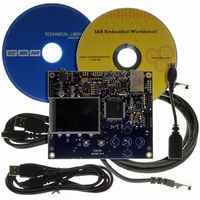
KIT EVAL FOR AT32UC3A0
Manufacturer
Atmel
Series
AVR®32r
Type
MCUr
Datasheets
1.ATAVRONE-PROBECBL.pdf
(16 pages)
2.ATEVK1104.pdf
(826 pages)
3.ATEVK1105.pdf
(28 pages)
Specifications of ATEVK1105
Contents
Evaluation Board, Software and Documentation
Processor To Be Evaluated
AT32UC3A0512
Processor Series
AVR
Data Bus Width
32 bit
Interface Type
USART, TWI, USB, SPI, Ethernet
Operating Supply Voltage
3.3 V
Silicon Manufacturer
Atmel
Core Architecture
AVR
Core Sub-architecture
AVR UC3
Silicon Core Number
AT32UC3A0512
Silicon Family Name
AVR
Kit Contents
Board CD Docs
Rohs Compliant
Yes
For Use With/related Products
AT32UC3A0
Lead Free Status / RoHS Status
Lead free / RoHS Compliant


36.9.2
32058J–AVR32–04/11
NEXUS_ACCESS
bold text. I.e. given the pattern " aaaaaaar xxxxxxxx xxxxxxxx xxxxxxxx xx", the shift register is
34 bits, but the test or debug unit may choose to shift only 8 bits " aaaaaaar ".
The following describes how to interpret the fields in the instruction description tables:
Table 36-4.
This instruction allows Nexus-compliant access to on-chip debug registers through the SAB.
OCD registers are addressed by their register index, as listed in the AVR32 Technical Reference
Manual. The 7-bit register index and a read/write control bit, and the 32-bit data is accessed
through the JTAG port.
The data register is alternately interpreted by the SAB as an address register and a data regis-
ter. The SAB starts in address mode after the NEXUS_ACCESS instruction is selected, and
toggles between address and data mode each time a data scan completes with the busy bit
cleared.
Starting in Run-Test/Idle, OCD registers are accessed in the following way:
Instruction
IR input value
IR output value
DR Size
DR input value
DR output value
1. Select the DR Scan path.
2. Scan in the 7-bit address for the OCD register and a direction bit (1=read, 0=write).
3. Go to Update-DR and re-enter Select-DR Scan.
4. For a read operation, scan out the contents of the addressed register. For a write oper-
5. Return to Run-Test/Idle.
ation, scan in the new contents of the register.
Instruction description
Description
Shows the bit pattern to shift into IR in the Shift-IR state in order to select this
instruction. The pattern is show both in binary and in hexadecimal form for
convenience.
Example: 10000 (0x10)
Shows the bit pattern shifted out of IR in the Shift-IR state when this instruction is
active.
Example: peb01
Shows the number of bits in the data register chain when this instruction is active.
Example: 34 bits
Shows which bit pattern to shift into the data register in the Shift-DR state when this
instruction is active. Multiple such lines may exist, e.g. to distinguish between reads
and writes.
Example: aaaaaaar xxxxxxxx xxxxxxxx xxxxxxxx xx
Shows the bit pattern shifted out of the data register in the Shift-DR state when this
instruction is active. Multiple such lines may exist, e.g. to distinguish between reads
and writes.
Example: xx xxxxxxxx xxxxxxxx xxxxxxxx xxxxxxeb
AT32UC3A
751
Related parts for ATEVK1105
Image
Part Number
Description
Manufacturer
Datasheet
Request
R

Part Number:
Description:
DEV KIT FOR AVR/AVR32
Manufacturer:
Atmel
Datasheet:

Part Number:
Description:
INTERVAL AND WIPE/WASH WIPER CONTROL IC WITH DELAY
Manufacturer:
ATMEL Corporation
Datasheet:
Part Number:
Description:
Low-Voltage Voice-Switched IC for Hands-Free Operation
Manufacturer:
ATMEL Corporation
Datasheet:
Part Number:
Description:
MONOLITHIC INTEGRATED FEATUREPHONE CIRCUIT
Manufacturer:
ATMEL Corporation
Datasheet:
Part Number:
Description:
AM-FM Receiver IC U4255BM-M
Manufacturer:
ATMEL Corporation
Datasheet:
Part Number:
Description:
Monolithic Integrated Feature Phone Circuit
Manufacturer:
ATMEL Corporation
Datasheet:
Part Number:
Description:
Multistandard Video-IF and Quasi Parallel Sound Processing
Manufacturer:
ATMEL Corporation
Datasheet:
Part Number:
Description:
High-performance EE PLD
Manufacturer:
ATMEL Corporation
Datasheet:
Part Number:
Description:
8-bit Flash Microcontroller
Manufacturer:
ATMEL Corporation
Datasheet:
Part Number:
Description:
2-Wire Serial EEPROM
Manufacturer:
ATMEL Corporation
Datasheet: