ATEVK1105 Atmel, ATEVK1105 Datasheet - Page 115
ATEVK1105
Manufacturer Part Number
ATEVK1105
Description
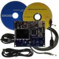
KIT EVAL FOR AT32UC3A0
Manufacturer
Atmel
Series
AVR®32r
Type
MCUr
Datasheets
1.ATAVRONE-PROBECBL.pdf
(16 pages)
2.ATEVK1104.pdf
(826 pages)
3.ATEVK1105.pdf
(28 pages)
Specifications of ATEVK1105
Contents
Evaluation Board, Software and Documentation
Processor To Be Evaluated
AT32UC3A0512
Processor Series
AVR
Data Bus Width
32 bit
Interface Type
USART, TWI, USB, SPI, Ethernet
Operating Supply Voltage
3.3 V
Silicon Manufacturer
Atmel
Core Architecture
AVR
Core Sub-architecture
AVR UC3
Silicon Core Number
AT32UC3A0512
Silicon Family Name
AVR
Kit Contents
Board CD Docs
Rohs Compliant
Yes
For Use With/related Products
AT32UC3A0
Lead Free Status / RoHS Status
Lead free / RoHS Compliant


18. Flash Controller (FLASHC)
18.1
18.2
18.3
18.3.1
18.3.2
32058J–AVR32–04/11
Features
Description
Product dependencies
Power management
Interrupt
Rev: 2.0.0.2
•
•
•
•
•
•
•
•
•
•
•
•
•
The flash controller (FLASHC) interfaces a flash block with the 32-bit internal HSB bus. Perfor-
mance for uncached systems with high clock-frequency and one wait state is increased by
placing words with sequential addresses in alternating flash subblocks. Having one read inter-
face per subblock allows them to be read in parallel. While data from one flash subblock is
being output on the bus, the sequential address is being read from the other flash subblock
and will be ready in the next clock cycle.
The controller also manages the programming, erasing, locking and unlocking sequences with
dedicated commands.
T h e H F L A S H C h a s t w o b u s c l o c k s c o n n e c t e d : O n e H i g h s p e e d b u s c l o c k
(CLK_FLASHC_HSB) and one Peripheral bus clock (CLK_FLASHC_PB). These clocks are
generated by the Power manager. Both clocks are turned on by default, but the user has to
ensure that CLK_FLASHC_HSB is not turned off before reading the flash or writing the page-
buffer and that CLK_FLASHC_PB is not turned of before accessing the FLASHC configuration
and control registers.
The FLASHC interrupt lines are connected to internal sources of the interrupt controller. Using
FLASHC interrutps requires the interrupt controller to be programmed first.
Controls flash block with dual read ports allowing staggered reads.
Supports 0 and 1 wait state bus access.
Allows interleaved burst reads for systems with one wait state, outputting one 32-bit word per
clock cycle.
32-bit HSB interface for reads from flash array and writes to page buffer.
32-bit PB interface for issuing commands to and configuration of the controller.
16 lock bits, each protecting a region consisting of (total number of pages in the flash block /
16) pages.
Regions can be individually protected or unprotected.
Additional protection of the Boot Loader pages.
Supports reads and writes of general-purpose NVM bits.
Supports reads and writes of additional NVM pages.
Supports device protection through a security bit.
Dedicated command for chip-erase, first erasing all on-chip volatile memories before erasing
flash and clearing security bit.
Interface to Power Manager for power-down of flash-blocks in sleep mode.
AT32UC3A
115
Related parts for ATEVK1105
Image
Part Number
Description
Manufacturer
Datasheet
Request
R

Part Number:
Description:
DEV KIT FOR AVR/AVR32
Manufacturer:
Atmel
Datasheet:

Part Number:
Description:
INTERVAL AND WIPE/WASH WIPER CONTROL IC WITH DELAY
Manufacturer:
ATMEL Corporation
Datasheet:
Part Number:
Description:
Low-Voltage Voice-Switched IC for Hands-Free Operation
Manufacturer:
ATMEL Corporation
Datasheet:
Part Number:
Description:
MONOLITHIC INTEGRATED FEATUREPHONE CIRCUIT
Manufacturer:
ATMEL Corporation
Datasheet:
Part Number:
Description:
AM-FM Receiver IC U4255BM-M
Manufacturer:
ATMEL Corporation
Datasheet:
Part Number:
Description:
Monolithic Integrated Feature Phone Circuit
Manufacturer:
ATMEL Corporation
Datasheet:
Part Number:
Description:
Multistandard Video-IF and Quasi Parallel Sound Processing
Manufacturer:
ATMEL Corporation
Datasheet:
Part Number:
Description:
High-performance EE PLD
Manufacturer:
ATMEL Corporation
Datasheet:
Part Number:
Description:
8-bit Flash Microcontroller
Manufacturer:
ATMEL Corporation
Datasheet:
Part Number:
Description:
2-Wire Serial EEPROM
Manufacturer:
ATMEL Corporation
Datasheet: