ATEVK1105 Atmel, ATEVK1105 Datasheet - Page 173
ATEVK1105
Manufacturer Part Number
ATEVK1105
Description
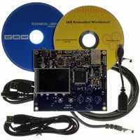
KIT EVAL FOR AT32UC3A0
Manufacturer
Atmel
Series
AVR®32r
Type
MCUr
Datasheets
1.ATAVRONE-PROBECBL.pdf
(16 pages)
2.ATEVK1104.pdf
(826 pages)
3.ATEVK1105.pdf
(28 pages)
Specifications of ATEVK1105
Contents
Evaluation Board, Software and Documentation
Processor To Be Evaluated
AT32UC3A0512
Processor Series
AVR
Data Bus Width
32 bit
Interface Type
USART, TWI, USB, SPI, Ethernet
Operating Supply Voltage
3.3 V
Silicon Manufacturer
Atmel
Core Architecture
AVR
Core Sub-architecture
AVR UC3
Silicon Core Number
AT32UC3A0512
Silicon Family Name
AVR
Kit Contents
Board CD Docs
Rohs Compliant
Yes
For Use With/related Products
AT32UC3A0
Lead Free Status / RoHS Status
Lead free / RoHS Compliant


22.4.7
22.4.8
22.4.9
32058J–AVR32–04/11
Interrupts
Input Glitch Filter
Interrupt Timings
Figure 22-2. Output line timings
The GPIO can be programmed to generate an interrupt when it detects an input change on an
I/O line. The module can be configured to signal an interrupt whenever a pin changes value or
only to trigger on rising edges or falling edges. Interrupt is enabled on a pin by setting the corre-
sponding bit in IER (Interrupt Enable Register). The interrupt mode is set by accessing IMR0
(Interrupt Mode Register 0) and IMR1 (Interrupt Mode Register 1). Interrupt can be enabled on a
pin, regardless of the configuration the I/O line, i.e. controlled by the GPIO or assigned to a
peripheral function.
In every port there are four interrupt lines connected to the interrupt controller. Every eigth inter-
rupts in the port are ored together to form an interrupt line.
When an interrupt event is detected on an I/O line, and the corresponding bit in IER is set, the
GPIO interrupt request line is asserted. A number of interrupt signals are ORed-wired together
to generate a single interrupt signal to the interrupt controller.
IFR (Interrupt Flag Register) can by read by software to determine which pin(s) caused the inter-
rupt. The interrupt flag must be manually cleared by writing to IFR.
GPIO interrupts can only be triggered when the GPIO clock is enabled.
Optional input glitch filters can be enabled on each I/O line. When the glitch filter is enabled, a
glitch with duration of less than 1 clock cycle is automatically rejected, while a pulse with dura-
tion of 2 clock cycles or more is accepted. For pulse durations between 1 clock cycle and 2 clock
cycles, the pulse may or may not be taken into account, depending on the precise timing of its
occurrence. Thus for a pulse to be guaranteed visible it must exceed 2 clock cycles, whereas for
a glitch to be reliably filtered out, its duration must not exceed 1 clock cycle. The filter introduces
2 clock cycles latency.
The glitch filters are controlled by the register GFER (Glitch Filter Enable Register). When a bit is
set in GFER, the glitch filter on the corresponding pin is enabled. The glitch filter affects only
interrupt inputs. Inputs to peripherals or the value read through PVR are not affected by the
glitch filters.
The figure below shows the timing for rising edge (or pin-change) interrupts when the glitch filter
is disabled. For the pulse to be registered, it must be sampled at the rising edge of the clock. In
this example, this is not the case for the first pulse. The second pulse is however sampled on a
rising edge and will trigger an interrupt request.
Write GPIO_OVR to 1
Write GPIO_OVR to 0
GPIO_OVR / I/O Line
GPIO_PVR
clock
PBA Access
PBA Access
AT32UC3A
173
Related parts for ATEVK1105
Image
Part Number
Description
Manufacturer
Datasheet
Request
R

Part Number:
Description:
DEV KIT FOR AVR/AVR32
Manufacturer:
Atmel
Datasheet:

Part Number:
Description:
INTERVAL AND WIPE/WASH WIPER CONTROL IC WITH DELAY
Manufacturer:
ATMEL Corporation
Datasheet:
Part Number:
Description:
Low-Voltage Voice-Switched IC for Hands-Free Operation
Manufacturer:
ATMEL Corporation
Datasheet:
Part Number:
Description:
MONOLITHIC INTEGRATED FEATUREPHONE CIRCUIT
Manufacturer:
ATMEL Corporation
Datasheet:
Part Number:
Description:
AM-FM Receiver IC U4255BM-M
Manufacturer:
ATMEL Corporation
Datasheet:
Part Number:
Description:
Monolithic Integrated Feature Phone Circuit
Manufacturer:
ATMEL Corporation
Datasheet:
Part Number:
Description:
Multistandard Video-IF and Quasi Parallel Sound Processing
Manufacturer:
ATMEL Corporation
Datasheet:
Part Number:
Description:
High-performance EE PLD
Manufacturer:
ATMEL Corporation
Datasheet:
Part Number:
Description:
8-bit Flash Microcontroller
Manufacturer:
ATMEL Corporation
Datasheet:
Part Number:
Description:
2-Wire Serial EEPROM
Manufacturer:
ATMEL Corporation
Datasheet: