ATEVK1105 Atmel, ATEVK1105 Datasheet - Page 33
ATEVK1105
Manufacturer Part Number
ATEVK1105
Description
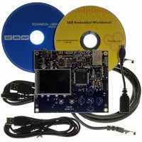
KIT EVAL FOR AT32UC3A0
Manufacturer
Atmel
Series
AVR®32r
Type
MCUr
Datasheets
1.ATAVRONE-PROBECBL.pdf
(16 pages)
2.ATEVK1104.pdf
(826 pages)
3.ATEVK1105.pdf
(28 pages)
Specifications of ATEVK1105
Contents
Evaluation Board, Software and Documentation
Processor To Be Evaluated
AT32UC3A0512
Processor Series
AVR
Data Bus Width
32 bit
Interface Type
USART, TWI, USB, SPI, Ethernet
Operating Supply Voltage
3.3 V
Silicon Manufacturer
Atmel
Core Architecture
AVR
Core Sub-architecture
AVR UC3
Silicon Core Number
AT32UC3A0512
Silicon Family Name
AVR
Kit Contents
Board CD Docs
Rohs Compliant
Yes
For Use With/related Products
AT32UC3A0
Lead Free Status / RoHS Status
Lead free / RoHS Compliant


10. Memories
10.1
10.2
Table 10-1.
32058J–AVR32–04/11
Device
Embedded SRAM
Embedded Flash
EBI SRAM CS0
EBI SRAM CS2
EBI SRAM CS3
EBI SRAM CS1
/SDRAM CS0
USB
Configuration
HSB-PB Bridge A
HSB-PB Bridge B
Embedded Memories
Physical Memory Map
AT32UC3A Physical Memory Map
Start Address
0x0000_0000
0x8000_0000
0xC000_0000
0xC800_0000
0xCC00_0000
0xD000_0000
0xE000_0000
0xFFFE_0000
0xFFFF_0000
•
•
The system bus is implemented as a bus matrix. All system bus addresses are fixed, and they
are never remapped in any way, not even in boot. Note that AVR32 UC CPU uses unsegmented
translation, as described in the AVR32 Architecture Manual. The 32-bit physical address space
is mapped as follows:
Internal High-Speed Flash
Internal High-Speed SRAM, Single-cycle access at full speed
– 512 KBytes (AT32UC3A0512, AT32UC3A1512)
– 256 KBytes (AT32UC3A0256, AT32UC3A1256)
– 128 KBytes (AT32UC3A1128, AT32UC3A2128)
– 64 KBytes (AT32UC3A0512, AT32UC3A0256, AT32UC3A1512, AT32UC3A1256)
– 32KBytes (AT32UC3A1128)
- 0 Wait State Access at up to 33 MHz in Worst Case Conditions
- 1 Wait State Access at up to 66 MHz in Worst Case Conditions
- Pipelined Flash Architecture, allowing burst reads from sequential Flash locations, hiding
penalty of 1 wait state access
- Pipelined Flash Architecture typically reduces the cycle penalty of 1 wait state operation
to only 15% compared to 0 wait state operation
- 100 000 Write Cycles, 15-year Data Retention Capability
- 4 ms Page Programming Time, 8 ms Chip Erase Time
- Sector Lock Capabilities, Bootloader Protection, Security Bit
- 32 Fuses, Erased During Chip Erase
- User Page For Data To Be Preserved During Chip Erase
Size
AT32UC3A0512
64 Kbyte
512 Kbyte
16 Mbyte
16 Mbyte
16 Mbyte
128 Mbyte
64 Kbyte
64 Kbyte
64 Kbyte
AT32UC3A1512
64 Kbyte
512 Kbyte
-
-
-
-
64 Kbyte
64 Kbyte
64 Kbyte
AT32UC3A0256
64 Kbyte
256 Kbyte
16 Mbyte
16 Mbyte
16 Mbyte
128 Mbyte
64 Kbyte
64 Kbyte
64 kByte
AT32UC3A1256
64 Kbyte
256 Kbyte
-
-
-
-
64 Kbyte
64 Kbyte
64 kByte
AT32UC3A0128
32 Kbyte
128 Kbyte
16 Mbyte
16 Mbyte
16 Mbyte
128 Mbyte
64 Kbyte
64 Kbyte
64 Kbyte
AT32UC3A
AT32UC3A1128
32 Kbyte
128 Kbyte
-
-
-
-
64 Kbyte
64 Kbyte
64 Kbyte
33
Related parts for ATEVK1105
Image
Part Number
Description
Manufacturer
Datasheet
Request
R

Part Number:
Description:
DEV KIT FOR AVR/AVR32
Manufacturer:
Atmel
Datasheet:

Part Number:
Description:
INTERVAL AND WIPE/WASH WIPER CONTROL IC WITH DELAY
Manufacturer:
ATMEL Corporation
Datasheet:
Part Number:
Description:
Low-Voltage Voice-Switched IC for Hands-Free Operation
Manufacturer:
ATMEL Corporation
Datasheet:
Part Number:
Description:
MONOLITHIC INTEGRATED FEATUREPHONE CIRCUIT
Manufacturer:
ATMEL Corporation
Datasheet:
Part Number:
Description:
AM-FM Receiver IC U4255BM-M
Manufacturer:
ATMEL Corporation
Datasheet:
Part Number:
Description:
Monolithic Integrated Feature Phone Circuit
Manufacturer:
ATMEL Corporation
Datasheet:
Part Number:
Description:
Multistandard Video-IF and Quasi Parallel Sound Processing
Manufacturer:
ATMEL Corporation
Datasheet:
Part Number:
Description:
High-performance EE PLD
Manufacturer:
ATMEL Corporation
Datasheet:
Part Number:
Description:
8-bit Flash Microcontroller
Manufacturer:
ATMEL Corporation
Datasheet:
Part Number:
Description:
2-Wire Serial EEPROM
Manufacturer:
ATMEL Corporation
Datasheet: