ATEVK1105 Atmel, ATEVK1105 Datasheet - Page 379
ATEVK1105
Manufacturer Part Number
ATEVK1105
Description
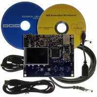
KIT EVAL FOR AT32UC3A0
Manufacturer
Atmel
Series
AVR®32r
Type
MCUr
Datasheets
1.ATAVRONE-PROBECBL.pdf
(16 pages)
2.ATEVK1104.pdf
(826 pages)
3.ATEVK1105.pdf
(28 pages)
Specifications of ATEVK1105
Contents
Evaluation Board, Software and Documentation
Processor To Be Evaluated
AT32UC3A0512
Processor Series
AVR
Data Bus Width
32 bit
Interface Type
USART, TWI, USB, SPI, Ethernet
Operating Supply Voltage
3.3 V
Silicon Manufacturer
Atmel
Core Architecture
AVR
Core Sub-architecture
AVR UC3
Silicon Core Number
AT32UC3A0512
Silicon Family Name
AVR
Kit Contents
Board CD Docs
Rohs Compliant
Yes
For Use With/related Products
AT32UC3A0
Lead Free Status / RoHS Status
Lead free / RoHS Compliant


32058J–AVR32–04/11
– Write Cycle
– Null Delay Setup and Hold
Figure 27-13. Write Cycle
The write_cycle time is defined as the total duration of the write cycle, that is, from the time
where address is set on the address bus to the point where address may change. The total write
cycle time is equal to:
NWE_CYCLE = NWE_SETUP + NWE_PULSE + NWE_HOLD
= NCS_WR_SETUP + NCS_WR_PULSE + NCS_WR_HOLD
All NWE and NCS (write) timings are defined separately for each chip select as an integer num-
ber of Master Clock cycles. To ensure that the NWE and NCS timings are coherent, the user
must define the total write cycle instead of the hold timing. This implicitly defines the NWE hold
time and NCS (write) hold times as:
NWE_HOLD = NWE_CYCLE - NWE_SETUP - NWE_PULSE
NCS_WR_HOLD = NWE_CYCLE - NCS_WR_SETUP - NCS_WR_PULSE
If null setup parameters are programmed for NWE and/or NCS, NWE and/or NCS remain active
continuously in case of consecutive write cycles in the same memory (see
ever, for devices that perform write operations on the rising edge of NWE or NCS, such as
SRAM, either a setup or a hold must be programmed.
NBS0, NBS1,
A0, A1
CLK_SMC
A[25:2]
NWE
NCS
NCS_WR_SETUP
NWE_SETUP
NCS_WR_PULSE
NWE_CYCLE
NWE_PULSE
NWE_HOLD
NCS_WR_HOLD
AT32UC3A
Figure
27-14). How-
379
Related parts for ATEVK1105
Image
Part Number
Description
Manufacturer
Datasheet
Request
R

Part Number:
Description:
DEV KIT FOR AVR/AVR32
Manufacturer:
Atmel
Datasheet:

Part Number:
Description:
INTERVAL AND WIPE/WASH WIPER CONTROL IC WITH DELAY
Manufacturer:
ATMEL Corporation
Datasheet:
Part Number:
Description:
Low-Voltage Voice-Switched IC for Hands-Free Operation
Manufacturer:
ATMEL Corporation
Datasheet:
Part Number:
Description:
MONOLITHIC INTEGRATED FEATUREPHONE CIRCUIT
Manufacturer:
ATMEL Corporation
Datasheet:
Part Number:
Description:
AM-FM Receiver IC U4255BM-M
Manufacturer:
ATMEL Corporation
Datasheet:
Part Number:
Description:
Monolithic Integrated Feature Phone Circuit
Manufacturer:
ATMEL Corporation
Datasheet:
Part Number:
Description:
Multistandard Video-IF and Quasi Parallel Sound Processing
Manufacturer:
ATMEL Corporation
Datasheet:
Part Number:
Description:
High-performance EE PLD
Manufacturer:
ATMEL Corporation
Datasheet:
Part Number:
Description:
8-bit Flash Microcontroller
Manufacturer:
ATMEL Corporation
Datasheet:
Part Number:
Description:
2-Wire Serial EEPROM
Manufacturer:
ATMEL Corporation
Datasheet: