ATEVK1105 Atmel, ATEVK1105 Datasheet - Page 439
ATEVK1105
Manufacturer Part Number
ATEVK1105
Description
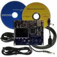
KIT EVAL FOR AT32UC3A0
Manufacturer
Atmel
Series
AVR®32r
Type
MCUr
Datasheets
1.ATAVRONE-PROBECBL.pdf
(16 pages)
2.ATEVK1104.pdf
(826 pages)
3.ATEVK1105.pdf
(28 pages)
Specifications of ATEVK1105
Contents
Evaluation Board, Software and Documentation
Processor To Be Evaluated
AT32UC3A0512
Processor Series
AVR
Data Bus Width
32 bit
Interface Type
USART, TWI, USB, SPI, Ethernet
Operating Supply Voltage
3.3 V
Silicon Manufacturer
Atmel
Core Architecture
AVR
Core Sub-architecture
AVR UC3
Silicon Core Number
AT32UC3A0512
Silicon Family Name
AVR
Kit Contents
Board CD Docs
Rohs Compliant
Yes
For Use With/related Products
AT32UC3A0
Lead Free Status / RoHS Status
Lead free / RoHS Compliant


29.4.3
29.5
29.5.1
29.5.1.1
32058J–AVR32–04/11
Functional Description
Interrupt
Memory Interface
FIFO
The MACB interface has an interrupt line connected to the Interrupt Controller. Handling the
MACB interrupt requires programming the interrupt controller before configuring the MACB.
Figure 29-1 on page 438
The control registers drive the MDIO interface, setup DMA activity, start frame transmission and
select modes of operation such as full- or half-duplex.
The receive block checks for valid preamble, FCS, alignment and length, and presents received
frames to the address checking block and DMA interface.
The transmit block takes data from the DMA interface, adds preamble and, if necessary, pad
and FCS, and transmits data according to the CSMA/CD (carrier sense multiple access with col-
lision detect) protocol. The start of transmission is deferred if CRS (carrier sense) is active.
If COL (collision) becomes active during transmission, a jam sequence is asserted and the
transmission is retried after a random back off. CRS and COL have no effect in full duplex mode.
The DMA block connects to external memory through its high speed bus (HSB) interface. It con-
tains receive and transmit FIFOs for buffering frame data. It loads the transmit FIFO and empties
the receive FIFO using HSB bus master operations. Receive data is not sent to memory until the
address checking logic has determined that the frame should be copied. Receive or transmit
frames are stored in one or more buffers. Receive buffers have a fixed length of 128 bytes.
Transmit buffers range in length between 0 and 2047 bytes, and up to 128 buffers are permitted
per frame. The DMA block manages the transmit and receive framebuffer queues. These
queues can hold multiple frames.
Frame data is transferred to and from the MACB through the DMA interface. All transfers are 32-
bit words and may be single accesses or bursts of 2, 3 or 4 words. Burst accesses do not cross
sixteen-byte boundaries. Bursts of 4 words are the default data transfer; single accesses or
bursts of less than four words may be used to transfer data at the beginning or the end of a
buffer.
The DMA controller performs six types of operation on the bus. In order of priority, these are:
The FIFO depths are 124 bytes.
Data is typically transferred into and out of the FIFOs in bursts of four words. For receive, a bus
request is asserted when the FIFO contains four words and has space for three more. For trans-
mit, a bus request is generated when there is space for four words, or when there is space for
two words if the next transfer is to be only one or two words.
1. Receive buffer manager write
2. Receive buffer manager read
3. Transmit data DMA read
4. Receive data DMA write
5. Transmit buffer manager read
6. Transmit buffer manager write
illustrates the different blocks of the MACB module.
AT32UC3A
439
Related parts for ATEVK1105
Image
Part Number
Description
Manufacturer
Datasheet
Request
R

Part Number:
Description:
DEV KIT FOR AVR/AVR32
Manufacturer:
Atmel
Datasheet:

Part Number:
Description:
INTERVAL AND WIPE/WASH WIPER CONTROL IC WITH DELAY
Manufacturer:
ATMEL Corporation
Datasheet:
Part Number:
Description:
Low-Voltage Voice-Switched IC for Hands-Free Operation
Manufacturer:
ATMEL Corporation
Datasheet:
Part Number:
Description:
MONOLITHIC INTEGRATED FEATUREPHONE CIRCUIT
Manufacturer:
ATMEL Corporation
Datasheet:
Part Number:
Description:
AM-FM Receiver IC U4255BM-M
Manufacturer:
ATMEL Corporation
Datasheet:
Part Number:
Description:
Monolithic Integrated Feature Phone Circuit
Manufacturer:
ATMEL Corporation
Datasheet:
Part Number:
Description:
Multistandard Video-IF and Quasi Parallel Sound Processing
Manufacturer:
ATMEL Corporation
Datasheet:
Part Number:
Description:
High-performance EE PLD
Manufacturer:
ATMEL Corporation
Datasheet:
Part Number:
Description:
8-bit Flash Microcontroller
Manufacturer:
ATMEL Corporation
Datasheet:
Part Number:
Description:
2-Wire Serial EEPROM
Manufacturer:
ATMEL Corporation
Datasheet: