DF2339VFC25V Renesas Electronics America, DF2339VFC25V Datasheet - Page 738
DF2339VFC25V
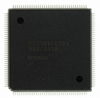
Manufacturer Part Number
DF2339VFC25V
Description
IC H8S/2300 MCU FLASH 144QFP
Manufacturer
Renesas Electronics America
Series
H8® H8S/2300r
Datasheets
1.HEWH8E10A.pdf
(19 pages)
2.D12312SVTE25V.pdf
(341 pages)
3.DF2338VFC25V.pdf
(1246 pages)
Specifications of DF2339VFC25V
Core Processor
H8S/2000
Core Size
16-Bit
Speed
25MHz
Connectivity
SCI, SmartCard
Peripherals
DMA, POR, PWM, WDT
Number Of I /o
106
Program Memory Size
384KB (384K x 8)
Program Memory Type
FLASH
Ram Size
32K x 8
Voltage - Supply (vcc/vdd)
3 V ~ 3.6 V
Data Converters
A/D 12x10b; D/A 4x8b
Oscillator Type
Internal
Operating Temperature
-20°C ~ 75°C
Package / Case
144-QFP
For Use With
EDK2329 - DEV EVALUATION KIT H8S/2329
Lead Free Status / RoHS Status
Lead free / RoHS Compliant
Eeprom Size
-
Available stocks
Company
Part Number
Manufacturer
Quantity
Price
Company:

Part Number:
DF2339VFC25V
Manufacturer:
Renesas Electronics America
Quantity:
10 000


CH3
0
1
16.2.3
ADCR is an 8-bit readable/writable register that enables or disables external triggering of A/D
conversion operations.
ADCR is initialized to H'3F by a reset, and in standby mode or module stop mode.
Bits 7 and 6—Timer Trigger Select 1 and 0 (TRGS1, TRGS0): These bits select enabling or
disabling of the start of A/D conversion by a trigger signal. Only set bits TRGS1 and TRGS0
while conversion is stopped (ADST = 0).
Rev.4.00 Sep. 07, 2007 Page 706 of 1210
REJ09B0245-0400
Bit
Initial value :
R/W
A/D Control Register (ADCR)
CH2
0
1
0
1
Channel Selection
:
:
TRGS1
R/W
7
0
CH1
0
1
0
1
0
1
0
1
TRGS0
R/W
6
0
CH0
0
1
0
1
0
1
0
1
0
1
0
1
0
1
0
1
—
—
5
1
Single Mode
(SCAN = 0)
AN12
AN13
AN15
AN1
AN3
AN4
AN5
AN7
Setting prohibited
AN14
AN0 (Initial value)
AN2
AN6
—
—
4
1
CKS1
R/W
1
3
Description
CH3
R/W
2
1
Scan Mode
(SCAN = 1)
Setting prohibited
AN12
AN12, AN13
AN12 to AN14
AN12 to AN15
AN0
AN0, AN1
AN0 to AN2
AN0 to AN3
AN4
AN4, AN5
AN4 to AN6
AN4 to AN7
—
—
1
1
—
—
0
1
Related parts for DF2339VFC25V
Image
Part Number
Description
Manufacturer
Datasheet
Request
R

Part Number:
Description:
KIT STARTER FOR M16C/29
Manufacturer:
Renesas Electronics America
Datasheet:

Part Number:
Description:
KIT STARTER FOR R8C/2D
Manufacturer:
Renesas Electronics America
Datasheet:

Part Number:
Description:
R0K33062P STARTER KIT
Manufacturer:
Renesas Electronics America
Datasheet:

Part Number:
Description:
KIT STARTER FOR R8C/23 E8A
Manufacturer:
Renesas Electronics America
Datasheet:

Part Number:
Description:
KIT STARTER FOR R8C/25
Manufacturer:
Renesas Electronics America
Datasheet:

Part Number:
Description:
KIT STARTER H8S2456 SHARPE DSPLY
Manufacturer:
Renesas Electronics America
Datasheet:

Part Number:
Description:
KIT STARTER FOR R8C38C
Manufacturer:
Renesas Electronics America
Datasheet:

Part Number:
Description:
KIT STARTER FOR R8C35C
Manufacturer:
Renesas Electronics America
Datasheet:

Part Number:
Description:
KIT STARTER FOR R8CL3AC+LCD APPS
Manufacturer:
Renesas Electronics America
Datasheet:
Part Number:
Description:
KIT STARTER FOR RX610
Manufacturer:
Renesas Electronics America
Datasheet:

Part Number:
Description:
KIT STARTER FOR R32C/118
Manufacturer:
Renesas Electronics America
Datasheet:

Part Number:
Description:
KIT DEV RSK-R8C/26-29
Manufacturer:
Renesas Electronics America
Datasheet:

Part Number:
Description:
KIT STARTER FOR SH7124
Manufacturer:
Renesas Electronics America
Datasheet:

Part Number:
Description:
KIT STARTER FOR H8SX/1622
Manufacturer:
Renesas Electronics America
Datasheet:

Part Number:
Description:
KIT DEV FOR SH7203
Manufacturer:
Renesas Electronics America
Datasheet: