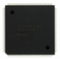
DF2339VFC25V Renesas Electronics America, DF2339VFC25V Datasheet - Page 175
DF2339VFC25V
Manufacturer Part Number
DF2339VFC25V
Description
IC H8S/2300 MCU FLASH 144QFP
Manufacturer
Renesas Electronics America
Series
H8® H8S/2300r
Datasheets
1.HEWH8E10A.pdf
(19 pages)
2.D12312SVTE25V.pdf
(341 pages)
3.DF2338VFC25V.pdf
(1246 pages)
Specifications of DF2339VFC25V
Core Processor
H8S/2000
Core Size
16-Bit
Speed
25MHz
Connectivity
SCI, SmartCard
Peripherals
DMA, POR, PWM, WDT
Number Of I /o
106
Program Memory Size
384KB (384K x 8)
Program Memory Type
FLASH
Ram Size
32K x 8
Voltage - Supply (vcc/vdd)
3 V ~ 3.6 V
Data Converters
A/D 12x10b; D/A 4x8b
Oscillator Type
Internal
Operating Temperature
-20°C ~ 75°C
Package / Case
144-QFP
For Use With
EDK2329 - DEV EVALUATION KIT H8S/2329
Lead Free Status / RoHS Status
Lead free / RoHS Compliant
Eeprom Size
-
Available stocks
Company
Part Number
Manufacturer
Quantity
Price
Company:

Part Number:
DF2339VFC25V
Manufacturer:
Renesas Electronics America
Quantity:
10 000


Bit 5
EAE
0
1
Notes: 1. Do not access a reserved area.
Bit 4—Reserved: Only 1 should be written to this bit.
Bit 3—DACK Timing Select (DDS): Selects the DMAC single address transfer bus timing for
the DRAM interface.
Bit 3
DDS
0
1
Bit 2—Reserved: Only 1 should be written to this bit.
Bit 1—Write Data Buffer Enable (WDBE): Selects whether or not the write buffer function is
used for an external write cycle or DMAC single address cycle.
Bit 1
WDBE
0
1
Bit 0—WAIT Pin Enable (WAITE): Selects enabling or disabling of wait input by the WAIT
pin.
Bit 0
WAITE
0
1
2. Addresses H'010000 to H'05FFFF in the H8S/2339.
On-chip ROM
Addresses H'010000 to H'03FFFF are external addresses in external expanded mode
or reserved area *
H8S/2339, H8S/2338
Description
When DMAC single address transfer is performed in DRAM space, full access is
always executed. DACK signal goes low from Tr or T1 cycle
Burst access is possible when DMAC single address transfer is performed in DRAM
space. DACK signal goes low from Tc1 or T2 cycle
Description
Write data buffer function not used
Write data buffer function used
Description
Wait input by WAIT pin disabled. WAIT pin can be used as I/O port
Wait input by WAIT pin enabled
1
in single-chip mode
on-chip ROM or addresses H'020000
to H'03FFFF are reserved area *
H8S/2337
Addresses H'010000 to H'01FFFF are
Description
Rev.4.00 Sep. 07, 2007 Page 143 of 1210
1
Reserved area *
H8S/2332
REJ09B0245-0400
(Initial value)
(Initial value)
(Initial value)
1
Related parts for DF2339VFC25V
Image
Part Number
Description
Manufacturer
Datasheet
Request
R

Part Number:
Description:
KIT STARTER FOR M16C/29
Manufacturer:
Renesas Electronics America
Datasheet:

Part Number:
Description:
KIT STARTER FOR R8C/2D
Manufacturer:
Renesas Electronics America
Datasheet:

Part Number:
Description:
R0K33062P STARTER KIT
Manufacturer:
Renesas Electronics America
Datasheet:

Part Number:
Description:
KIT STARTER FOR R8C/23 E8A
Manufacturer:
Renesas Electronics America
Datasheet:

Part Number:
Description:
KIT STARTER FOR R8C/25
Manufacturer:
Renesas Electronics America
Datasheet:

Part Number:
Description:
KIT STARTER H8S2456 SHARPE DSPLY
Manufacturer:
Renesas Electronics America
Datasheet:

Part Number:
Description:
KIT STARTER FOR R8C38C
Manufacturer:
Renesas Electronics America
Datasheet:

Part Number:
Description:
KIT STARTER FOR R8C35C
Manufacturer:
Renesas Electronics America
Datasheet:

Part Number:
Description:
KIT STARTER FOR R8CL3AC+LCD APPS
Manufacturer:
Renesas Electronics America
Datasheet:
Part Number:
Description:
KIT STARTER FOR RX610
Manufacturer:
Renesas Electronics America
Datasheet:

Part Number:
Description:
KIT STARTER FOR R32C/118
Manufacturer:
Renesas Electronics America
Datasheet:

Part Number:
Description:
KIT DEV RSK-R8C/26-29
Manufacturer:
Renesas Electronics America
Datasheet:

Part Number:
Description:
KIT STARTER FOR SH7124
Manufacturer:
Renesas Electronics America
Datasheet:

Part Number:
Description:
KIT STARTER FOR H8SX/1622
Manufacturer:
Renesas Electronics America
Datasheet:

Part Number:
Description:
KIT DEV FOR SH7203
Manufacturer:
Renesas Electronics America
Datasheet: