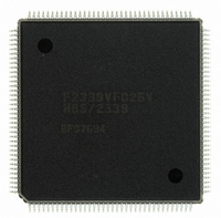
DF2339VFC25V Renesas Electronics America, DF2339VFC25V Datasheet - Page 369
DF2339VFC25V
Manufacturer Part Number
DF2339VFC25V
Description
IC H8S/2300 MCU FLASH 144QFP
Manufacturer
Renesas Electronics America
Series
H8® H8S/2300r
Datasheets
1.HEWH8E10A.pdf
(19 pages)
2.D12312SVTE25V.pdf
(341 pages)
3.DF2338VFC25V.pdf
(1246 pages)
Specifications of DF2339VFC25V
Core Processor
H8S/2000
Core Size
16-Bit
Speed
25MHz
Connectivity
SCI, SmartCard
Peripherals
DMA, POR, PWM, WDT
Number Of I /o
106
Program Memory Size
384KB (384K x 8)
Program Memory Type
FLASH
Ram Size
32K x 8
Voltage - Supply (vcc/vdd)
3 V ~ 3.6 V
Data Converters
A/D 12x10b; D/A 4x8b
Oscillator Type
Internal
Operating Temperature
-20°C ~ 75°C
Package / Case
144-QFP
For Use With
EDK2329 - DEV EVALUATION KIT H8S/2329
Lead Free Status / RoHS Status
Lead free / RoHS Compliant
Eeprom Size
-
Available stocks
Company
Part Number
Manufacturer
Quantity
Price
Company:

Part Number:
DF2339VFC25V
Manufacturer:
Renesas Electronics America
Quantity:
10 000


9.2.3
Port 1 pins also function as PPG output pins (PO
TCLKC, TCLKD, TIOCA
TIOCB
Table 9.3
Pin
P1
TIOCB
7
/PO
2
2
15
/TCLKD
) Port 1 pin functions are shown in table 9.3.
/
Pin Functions
Port 1 Pin Functions
Selection Method and Pin Functions
The pin function is switched as shown below according to the combination of
the TPU channel 2 setting (by bits MD3 to MD0 in TMDR2, bits IOB3 to IOB0
in TIOR2, and bits CCLR1 and CCLR0 in TCR2), bits TPSC2 to TPSC0 in
TCR0 and TCR5, bit NDER15 in NDERH, and bit P17DDR.
Notes: 1. TIOCB
TPU Channel
2 Setting
P17DDR
NDER15
Pin function
TPU Channel
2 Setting
MD3 to MD0
IOB3 to IOB0
CCLR1,
CCLR0
Output
function
0
, TIOCB
2. TCLKD input when the setting for either TCR0 or TCR5 is: TPSC2
to TPSC0 = B'111.
TCLKD input when channels 2 and 4 are set to phase counting
mode.
0
, TIOCC
B'0000
B'0100
B'1xxx
2
B'0000, B'01xx
input when MD3 to MD0 = B'0000 or B'01xx, and IOB3 = 1.
(2)
—
—
Table Below (1)
TIOCB
0
, TIOCD
B'0001 to
B'0011
B'0101 to
B'0111
compare
Output
output
15
(1)
—
—
—
to PO
2
output
0
Rev.4.00 Sep. 07, 2007 Page 337 of 1210
, TIOCA
8
) and TPU I/O pins (TCLKA, TCLKB,
B'0010
TCLKD input *
(2)
—
—
—
1
, TIOCB
B'xx00
input
P1
(2)
—
—
—
0
7
2
1
Table Below (2)
TIOCB
, TIOCA
than B'10
Other than B'xx00
mode 2
B'0011
output
output
REJ09B0245-0400
Other
PWM
P1
(1)
2
1
0
input *
7
2
, and
x: Don't care
1
output
PO
B'10
(2)
—
1
1
15
Related parts for DF2339VFC25V
Image
Part Number
Description
Manufacturer
Datasheet
Request
R

Part Number:
Description:
KIT STARTER FOR M16C/29
Manufacturer:
Renesas Electronics America
Datasheet:

Part Number:
Description:
KIT STARTER FOR R8C/2D
Manufacturer:
Renesas Electronics America
Datasheet:

Part Number:
Description:
R0K33062P STARTER KIT
Manufacturer:
Renesas Electronics America
Datasheet:

Part Number:
Description:
KIT STARTER FOR R8C/23 E8A
Manufacturer:
Renesas Electronics America
Datasheet:

Part Number:
Description:
KIT STARTER FOR R8C/25
Manufacturer:
Renesas Electronics America
Datasheet:

Part Number:
Description:
KIT STARTER H8S2456 SHARPE DSPLY
Manufacturer:
Renesas Electronics America
Datasheet:

Part Number:
Description:
KIT STARTER FOR R8C38C
Manufacturer:
Renesas Electronics America
Datasheet:

Part Number:
Description:
KIT STARTER FOR R8C35C
Manufacturer:
Renesas Electronics America
Datasheet:

Part Number:
Description:
KIT STARTER FOR R8CL3AC+LCD APPS
Manufacturer:
Renesas Electronics America
Datasheet:
Part Number:
Description:
KIT STARTER FOR RX610
Manufacturer:
Renesas Electronics America
Datasheet:

Part Number:
Description:
KIT STARTER FOR R32C/118
Manufacturer:
Renesas Electronics America
Datasheet:

Part Number:
Description:
KIT DEV RSK-R8C/26-29
Manufacturer:
Renesas Electronics America
Datasheet:

Part Number:
Description:
KIT STARTER FOR SH7124
Manufacturer:
Renesas Electronics America
Datasheet:

Part Number:
Description:
KIT STARTER FOR H8SX/1622
Manufacturer:
Renesas Electronics America
Datasheet:

Part Number:
Description:
KIT DEV FOR SH7203
Manufacturer:
Renesas Electronics America
Datasheet: