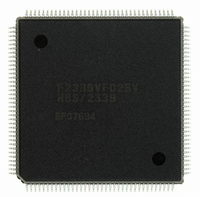
DF2339VFC25V Renesas Electronics America, DF2339VFC25V Datasheet - Page 185

DF2339VFC25V
Manufacturer Part Number
DF2339VFC25V
Description
IC H8S/2300 MCU FLASH 144QFP
Manufacturer
Renesas Electronics America
Series
H8® H8S/2300r
Datasheets
1.HEWH8E10A.pdf
(19 pages)
2.D12312SVTE25V.pdf
(341 pages)
3.DF2338VFC25V.pdf
(1246 pages)
Specifications of DF2339VFC25V
Core Processor
H8S/2000
Core Size
16-Bit
Speed
25MHz
Connectivity
SCI, SmartCard
Peripherals
DMA, POR, PWM, WDT
Number Of I /o
106
Program Memory Size
384KB (384K x 8)
Program Memory Type
FLASH
Ram Size
32K x 8
Voltage - Supply (vcc/vdd)
3 V ~ 3.6 V
Data Converters
A/D 12x10b; D/A 4x8b
Oscillator Type
Internal
Operating Temperature
-20°C ~ 75°C
Package / Case
144-QFP
For Use With
EDK2329 - DEV EVALUATION KIT H8S/2329
Lead Free Status / RoHS Status
Lead free / RoHS Compliant
Eeprom Size
-
Available stocks
Company
Part Number
Manufacturer
Quantity
Price
Company:
Part Number:
DF2339VFC25V
Manufacturer:
Renesas Electronics America
Quantity:
10 000
- Current page: 185 of 1246
- Download datasheet (7Mb)
6.3.5
The chip can output chip select signals (CS
when the corresponding external space area is accessed.
Figure 6.3 shows an example of CS
Enabling or disabling of CS
(DDR) bit for the port corresponding to the particular CS
the CS25 enable bit (CS25E).
In expanded mode with on-chip ROM disabled, the CS0 pin is placed in the output state after a
reset. Pins CS
well as bits CS/67E and CS25E should be set to 1 when outputting signals CS
In expanded mode with on-chip ROM enabled, pins CS
after a reset, so the corresponding DDR bits as well as bits CS/67E and CS25E should be set to 1
when outputting signals CS
For details, see section 9, I/O Ports.
When areas 2 to 5 are designated as DRAM space, outputs CS
Chip Select Signals
1
to CS
Address
bus
CS
φ
n
7
are placed in the input state after a reset, so the corresponding DDR bits as
Figure 6.3 CS
1
n
to CS
signal output is performed by setting the data direction register
7
.
n
(n = 0 to 7) output timing.
n
T
Signal Output Timing (n = 0 to 7)
1
Area n external address
0
to CS
Bus cycle
7
) to areas 0 to 7, the signal being driven low
T
2
0
Rev.4.00 Sep. 07, 2007 Page 153 of 1210
n
to CS
pin, the CS/67 enable bit (CS/67E), and
2
7
to CS
are all placed in the input state
T
3
5
are used as RAS signals.
1
to CS
REJ09B0245-0400
7
.
Related parts for DF2339VFC25V
Image
Part Number
Description
Manufacturer
Datasheet
Request
R

Part Number:
Description:
KIT STARTER FOR M16C/29
Manufacturer:
Renesas Electronics America
Datasheet:

Part Number:
Description:
KIT STARTER FOR R8C/2D
Manufacturer:
Renesas Electronics America
Datasheet:

Part Number:
Description:
R0K33062P STARTER KIT
Manufacturer:
Renesas Electronics America
Datasheet:

Part Number:
Description:
KIT STARTER FOR R8C/23 E8A
Manufacturer:
Renesas Electronics America
Datasheet:

Part Number:
Description:
KIT STARTER FOR R8C/25
Manufacturer:
Renesas Electronics America
Datasheet:

Part Number:
Description:
KIT STARTER H8S2456 SHARPE DSPLY
Manufacturer:
Renesas Electronics America
Datasheet:

Part Number:
Description:
KIT STARTER FOR R8C38C
Manufacturer:
Renesas Electronics America
Datasheet:

Part Number:
Description:
KIT STARTER FOR R8C35C
Manufacturer:
Renesas Electronics America
Datasheet:

Part Number:
Description:
KIT STARTER FOR R8CL3AC+LCD APPS
Manufacturer:
Renesas Electronics America
Datasheet:

Part Number:
Description:
KIT STARTER FOR RX610
Manufacturer:
Renesas Electronics America
Datasheet:

Part Number:
Description:
KIT STARTER FOR R32C/118
Manufacturer:
Renesas Electronics America
Datasheet:

Part Number:
Description:
KIT DEV RSK-R8C/26-29
Manufacturer:
Renesas Electronics America
Datasheet:

Part Number:
Description:
KIT STARTER FOR SH7124
Manufacturer:
Renesas Electronics America
Datasheet:

Part Number:
Description:
KIT STARTER FOR H8SX/1622
Manufacturer:
Renesas Electronics America
Datasheet:

Part Number:
Description:
KIT DEV FOR SH7203
Manufacturer:
Renesas Electronics America
Datasheet:


