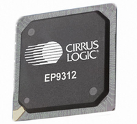
EP9312-CB Cirrus Logic Inc, EP9312-CB Datasheet - Page 658

EP9312-CB
Manufacturer Part Number
EP9312-CB
Description
System-on-Chip Processor
Manufacturer
Cirrus Logic Inc
Series
EP9r
Datasheets
1.EP9307-CRZ.pdf
(824 pages)
2.EP9312-IBZ.pdf
(4 pages)
3.EP9312-CB.pdf
(62 pages)
4.EP9312-CB.pdf
(17 pages)
Specifications of EP9312-CB
Peak Reflow Compatible (260 C)
No
A/d Converter
12 Bits
Leaded Process Compatible
No
No. Of I/o Pins
65
Package / Case
352-BGA
Core Processor
ARM9
Core Size
16/32-Bit
Speed
200MHz
Connectivity
EBI/EMI, EIDE, Ethernet, I²C, IrDA, Keypad/Touchscreen, SPI, UART/USART, USB
Peripherals
AC'97, DMA, I²:S, LCD, LED, MaverickKey, POR, PWM, WDT
Number Of I /o
16
Program Memory Type
ROMless
Ram Size
32K x 8
Voltage - Supply (vcc/vdd)
1.65 V ~ 3.6 V
Data Converters
A/D 8x12b
Oscillator Type
External
Operating Temperature
0°C ~ 70°C
Processor Series
EP93xx
Core
ARM920T
Data Bus Width
32 bit
3rd Party Development Tools
MDK-ARM, RL-ARM, ULINK2
Lead Free Status / RoHS Status
Contains lead / RoHS non-compliant
Eeprom Size
-
Program Memory Size
-
Lead Free Status / Rohs Status
No
Other names
598-1257
Available stocks
Company
Part Number
Manufacturer
Quantity
Price
Part Number:
EP9312-CB
Manufacturer:
CIRRUS
Quantity:
20 000
- EP9307-CRZ PDF datasheet
- EP9312-IBZ PDF datasheet #2
- EP9312-CB PDF datasheet #3
- EP9312-CB PDF datasheet #4
- Current page: 658 of 824
- Download datasheet (13Mb)
21
21-2
I
EP93xx User’s Guide
21.2 I
2
S Controller
The primary I
SSP pins or the Ac97 pins. The second and third I
primary I
second I
EGPIO[5] respectively and are enabled by setting DeviceCfg.A1onG. The third I
serial output and serial input pins are multiplexed with EGPIO[6] and EGPIO[13] respectively
and are enabled by setting DeviceCfg.A2onG.
Each I
can operate in master or slave mode. Data is transferred between the ARM Core and the I
controller via an interrupt based mechanism or DMA access. The ARM Core or host
processor must write words in multiples of 2 (that is, a left and right stereo pair). These words
are serially shifted out, timed with respect to the audio bit clock and word clock (SCLK and
LRCK) that are generated (see
The key features of the I
2
• Three transmit data channels, master or slave mode.
S Transmitter Channel Overview
2
S TX channel provides a single stereo I
2
2
S port's serial output and serial input pins are multiplexed with EGPIO[4] and
S port, but their serial output and input pins are multiplexed with EGPIO pins. The
ABITCLK
SSPRX1
SSPTX1
SFRM1
ASYNC
SCLK1
ARSTn
Name
ASDO
ASDI
Pin
2
Signal Name
S port and the I
sdo0
sdo1
sdo2
sdi0
sdi1
sdi2
lrck
sck
AC'97 Serial Output
AC'97 Frame Clock
Pin Description
AC'97 Serial Input
SPI Serial Output
SPI Frame Clock
Normal Mode
SPI Serial Input
AC'97 Bit Clock
2
Table 21-1. I
SPI Bit Clock
AC'97 Reset
S transmitter are:
Table 21-2. Audio Interfaces Pin Assignment
2
Copyright 2007 Cirrus Logic
S clocks are multiplexed and can be assigned to either the
Chapter
Type
OUT
OUT
OUT
IN
IN
IN
IN
IN
2
S Controller Input and Output Signals
5,
Left/right Word Audio slave clock.
Audio bit slave clock.
Serial data for channel 0
Serial data for channel 1
Serial data for channel 2
Serial data output for TX channel 0
Serial data output for TX channel 1
Serial data output for TX channel 2
“Clock Control” on page 5-4
(No I
I
AC'97 Serial Output
AC'97 Frame Clock
2
Pin Description
AC'97 Serial Input
I
S on SSP Mode
I
I
2
AC'97 Bit Clock
2
I
2
2
S Serial Output
S Frame Clock
S Serial Clock
AC'97 Reset
S Serial Input
2
2
S Master Clock)
S compliant output. The Transmit channel
2
S ports use the same clock pins as the
Description
I
2
S on AC'97 Mode
Pin Description
SPI Serial Output
SPI Frame Clock
I
I
I
I
SPI Serial Input
2
2
2
I
2
S Master Clock
2
S Serial Output
SPI Bit Clock
S Frame Clock
S Serial Clock
S Serial Input
for additional details).
2
S port's
DS785UM1
2
S
Related parts for EP9312-CB
Image
Part Number
Description
Manufacturer
Datasheet
Request
R

Part Number:
Description:
IC ARM920T MCU 200MHZ 352-PBGA
Manufacturer:
Cirrus Logic Inc
Datasheet:

Part Number:
Description:
IC ARM9 SOC UNIVERSAL 352PBGA
Manufacturer:
Cirrus Logic Inc
Datasheet:

Part Number:
Description:
IC ARM920T MCU 200MHZ 352-PBGA
Manufacturer:
Cirrus Logic Inc
Datasheet:

Part Number:
Description:
IC Universal Platform ARM9 SOC Prcessor
Manufacturer:
Cirrus Logic Inc
Datasheet:

Part Number:
Description:
IC Universal Platform ARM9 SOC Prcessor
Manufacturer:
Cirrus Logic Inc
Datasheet:

Part Number:
Description:
Development Kit
Manufacturer:
Cirrus Logic Inc
Datasheet:

Part Number:
Description:
Development Kit
Manufacturer:
Cirrus Logic Inc
Datasheet:

Part Number:
Description:
High-efficiency PFC + Fluorescent Lamp Driver Reference Design
Manufacturer:
Cirrus Logic Inc
Datasheet:

Part Number:
Description:
Development Kit
Manufacturer:
Cirrus Logic Inc
Datasheet:

Part Number:
Description:
Development Kit
Manufacturer:
Cirrus Logic Inc
Datasheet:

Part Number:
Description:
Development Kit
Manufacturer:
Cirrus Logic Inc
Datasheet:

Part Number:
Description:
Development Kit
Manufacturer:
Cirrus Logic Inc
Datasheet:

Part Number:
Description:
Ref Bd For Speakerbar MSA & DSP Products
Manufacturer:
Cirrus Logic Inc


