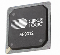
EP9312-CB Cirrus Logic Inc, EP9312-CB Datasheet - Page 215

EP9312-CB
Manufacturer Part Number
EP9312-CB
Description
System-on-Chip Processor
Manufacturer
Cirrus Logic Inc
Series
EP9r
Datasheets
1.EP9307-CRZ.pdf
(824 pages)
2.EP9312-IBZ.pdf
(4 pages)
3.EP9312-CB.pdf
(62 pages)
4.EP9312-CB.pdf
(17 pages)
Specifications of EP9312-CB
Peak Reflow Compatible (260 C)
No
A/d Converter
12 Bits
Leaded Process Compatible
No
No. Of I/o Pins
65
Package / Case
352-BGA
Core Processor
ARM9
Core Size
16/32-Bit
Speed
200MHz
Connectivity
EBI/EMI, EIDE, Ethernet, I²C, IrDA, Keypad/Touchscreen, SPI, UART/USART, USB
Peripherals
AC'97, DMA, I²:S, LCD, LED, MaverickKey, POR, PWM, WDT
Number Of I /o
16
Program Memory Type
ROMless
Ram Size
32K x 8
Voltage - Supply (vcc/vdd)
1.65 V ~ 3.6 V
Data Converters
A/D 8x12b
Oscillator Type
External
Operating Temperature
0°C ~ 70°C
Processor Series
EP93xx
Core
ARM920T
Data Bus Width
32 bit
3rd Party Development Tools
MDK-ARM, RL-ARM, ULINK2
Lead Free Status / RoHS Status
Contains lead / RoHS non-compliant
Eeprom Size
-
Program Memory Size
-
Lead Free Status / Rohs Status
No
Other names
598-1257
Available stocks
Company
Part Number
Manufacturer
Quantity
Price
Part Number:
EP9312-CB
Manufacturer:
CIRRUS
Quantity:
20 000
- EP9307-CRZ PDF datasheet
- EP9312-IBZ PDF datasheet #2
- EP9312-CB PDF datasheet #3
- EP9312-CB PDF datasheet #4
- Current page: 215 of 824
- Download datasheet (13Mb)
DS785UM1
7.4.11.2.1 PattrnMask Register
7.4.11.2.2 BlinkPattrn Register
7.4.11.2.3 BlinkMask Register
7.4.11.3 Types of Blinking
This register defines which bits in a pixel are blink bits. To enable an individual bit for
comparison requires setting that corresponding bit to “1”. To disable an individual bit for
comparison set the bit position to “0”.
For example, in 8bpp mode, the PattrnMask is defined as 0x0000_0080. This means that the
MSB of a pixel is used to assist is defined as a blink bit.
The
The pixel value is first masked by the PattrnMask value in the
result is compared to BlinkPattrn value in the
in a match, the pixel is considered to be a valid blink pixel.
For example:
An 8-bit pixel is defined as 0xAF (0b1010_1111b).
PattrnMask is defined as 0x0000_00C0.
BlinkPattrn is defined as 0x0000_0080.
PattrnMask = 0xC0 defines the two MSBs of 8-bit pixels as potential blink bits. If the two
corresponding MSBs in the BlinkPattrn register are ‘10’ and the two MSBs of the pixel value
are ‘10’, then the pixel of value = 0xAF is a blink pixel. In fact, all pixel values of 10xx_xxxx
are blink pixels. If BlinkPattrn was changed to 0x0000_0048 above, a pixel of value 0xAF
would not be a blink pixel.
The
“PixelMode”
register is ANDed (clearing bits), ORed (setting bits), or XORed (inverting bits) with a pixel
that addresses the LUT. The mask allows a blinking pixel to jump from a normal color
definition location to a blink color definition location in the LUT.
Once a pixel has been defined as a blink pixel, it is necessary to provide information on how
that pixel will blink. The blink type provides determines what operations are performed on the
pixel data as it moves through the blink logic to transform it into a blinking pixel.
There are 10 ways to blink a pixel once it has been defined as a blinking pixel. The blink type
is defined by the M[3:0] bits in the
0000 - Blink Disabled
0001 - AND Blinking.
“BlinkPattrn”
“BlinkMask”
continue through the pipeline.
The pixel data is ANDed with the
LUT Blink:
register are set for an AND, OR, or XOR operation. The value in the
register is only used if the blink mode definition bits M[3:0] in the
register is used to further refine which pixel pattern defines a blink pixel.
Copyright 2007 Cirrus Logic
“PixelMode”
Raster Engine With Analog/LCD Integrated Timing and Interface
“BlinkMask”
“BlinkPattrn”
register:
register. The modified pixel data will
register. If the comparison results
“PattrnMask”
EP93xx User’s Guide
register and the
“BlinkMask”
7-33
7
Related parts for EP9312-CB
Image
Part Number
Description
Manufacturer
Datasheet
Request
R

Part Number:
Description:
IC ARM920T MCU 200MHZ 352-PBGA
Manufacturer:
Cirrus Logic Inc
Datasheet:

Part Number:
Description:
IC ARM9 SOC UNIVERSAL 352PBGA
Manufacturer:
Cirrus Logic Inc
Datasheet:

Part Number:
Description:
IC ARM920T MCU 200MHZ 352-PBGA
Manufacturer:
Cirrus Logic Inc
Datasheet:

Part Number:
Description:
IC Universal Platform ARM9 SOC Prcessor
Manufacturer:
Cirrus Logic Inc
Datasheet:

Part Number:
Description:
IC Universal Platform ARM9 SOC Prcessor
Manufacturer:
Cirrus Logic Inc
Datasheet:

Part Number:
Description:
Development Kit
Manufacturer:
Cirrus Logic Inc
Datasheet:

Part Number:
Description:
Development Kit
Manufacturer:
Cirrus Logic Inc
Datasheet:

Part Number:
Description:
High-efficiency PFC + Fluorescent Lamp Driver Reference Design
Manufacturer:
Cirrus Logic Inc
Datasheet:

Part Number:
Description:
Development Kit
Manufacturer:
Cirrus Logic Inc
Datasheet:

Part Number:
Description:
Development Kit
Manufacturer:
Cirrus Logic Inc
Datasheet:

Part Number:
Description:
Development Kit
Manufacturer:
Cirrus Logic Inc
Datasheet:

Part Number:
Description:
Development Kit
Manufacturer:
Cirrus Logic Inc
Datasheet:

Part Number:
Description:
Ref Bd For Speakerbar MSA & DSP Products
Manufacturer:
Cirrus Logic Inc


