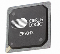
EP9312-CB Cirrus Logic Inc, EP9312-CB Datasheet - Page 274

EP9312-CB
Manufacturer Part Number
EP9312-CB
Description
System-on-Chip Processor
Manufacturer
Cirrus Logic Inc
Series
EP9r
Datasheets
1.EP9307-CRZ.pdf
(824 pages)
2.EP9312-IBZ.pdf
(4 pages)
3.EP9312-CB.pdf
(62 pages)
4.EP9312-CB.pdf
(17 pages)
Specifications of EP9312-CB
Peak Reflow Compatible (260 C)
No
A/d Converter
12 Bits
Leaded Process Compatible
No
No. Of I/o Pins
65
Package / Case
352-BGA
Core Processor
ARM9
Core Size
16/32-Bit
Speed
200MHz
Connectivity
EBI/EMI, EIDE, Ethernet, I²C, IrDA, Keypad/Touchscreen, SPI, UART/USART, USB
Peripherals
AC'97, DMA, I²:S, LCD, LED, MaverickKey, POR, PWM, WDT
Number Of I /o
16
Program Memory Type
ROMless
Ram Size
32K x 8
Voltage - Supply (vcc/vdd)
1.65 V ~ 3.6 V
Data Converters
A/D 8x12b
Oscillator Type
External
Operating Temperature
0°C ~ 70°C
Processor Series
EP93xx
Core
ARM920T
Data Bus Width
32 bit
3rd Party Development Tools
MDK-ARM, RL-ARM, ULINK2
Lead Free Status / RoHS Status
Contains lead / RoHS non-compliant
Eeprom Size
-
Program Memory Size
-
Lead Free Status / Rohs Status
No
Other names
598-1257
Available stocks
Company
Part Number
Manufacturer
Quantity
Price
Part Number:
EP9312-CB
Manufacturer:
CIRRUS
Quantity:
20 000
- EP9307-CRZ PDF datasheet
- EP9312-IBZ PDF datasheet #2
- EP9312-CB PDF datasheet #3
- EP9312-CB PDF datasheet #4
- Current page: 274 of 824
- Download datasheet (13Mb)
8
8-10
Graphics Accelerator
EP93xx User’s Guide
8.5.2.1 4 BPP Word Layout
memory and the other register, “DESTPIXELSTRT”, is used for the destination memory. All
start and stop values described below apply for source and destination values.
The two registers operate in an identical fashion for source and destination. To see how they
operate requires looking at several tables that show the memory layout for pixels in the
various color modes.
This 4 BPP mode example is somewhat difficult because the pixels are not in sequential
order. For a Block Copy where 8 pixels are transferred per scan line, let the starting SDRAM
address of the source image be 0x0000.
starts at bit 0, etc. The start pixel, P0, is in the word at address 0x0000 and has a beginning
bit position of 4. This makes 4 = 0x4 the value that is used for the SPEL field in the
“SRCPIXELSTRT”
Let the starting SDRAM address of the destination image be 0x0020.
Pixel 0 starts at bit 20, Pixel 1 starts at bit 16, etc. The start pixel, P0, is in the word at address
0x0020 and has a beginning bit position of 20. This makes 20 = 0x14 the value that is used
for the SPEL field in the
The end pixel, P7, is in the word at address 0x0024 and has a beginning bit position of 8. This
makes 8 = 0x8 the value that is used for the EPEL field in the
Note:The word count for this example would be: 2 - 1 = 1 words, since P7 ends in the 2nd word.
Address
Address
0x0000
0x0020
0x0024
So, WIDTH = 0x1 would be written to the
31
31
P6
P2
Table 8-14. 4 BPP Memory Layout for Destination Image
register.
28 27
28 27
Table 8-13. 4 BPP Memory Layout for Source Image
“DESTPIXELSTRT”
P7
P3
24 23
24 23
Copyright 2007 Cirrus Logic
P4
P0
20 19
20 19
Table 8-13
P5
P1
“BLKDESTWIDTH”
register.
16 15
16 15
P2
P6
shows that Pixel 0 starts at bit 4, Pixel 1
12 11
12 11
P3
P7
“DESTPIXELSTRT”
register.
8 7
8 7
P0
P4
Table 8-14
4 3
4 3
P1
P5
0
0
shows that
register.
DS785UM1
Related parts for EP9312-CB
Image
Part Number
Description
Manufacturer
Datasheet
Request
R

Part Number:
Description:
IC ARM920T MCU 200MHZ 352-PBGA
Manufacturer:
Cirrus Logic Inc
Datasheet:

Part Number:
Description:
IC ARM9 SOC UNIVERSAL 352PBGA
Manufacturer:
Cirrus Logic Inc
Datasheet:

Part Number:
Description:
IC ARM920T MCU 200MHZ 352-PBGA
Manufacturer:
Cirrus Logic Inc
Datasheet:

Part Number:
Description:
IC Universal Platform ARM9 SOC Prcessor
Manufacturer:
Cirrus Logic Inc
Datasheet:

Part Number:
Description:
IC Universal Platform ARM9 SOC Prcessor
Manufacturer:
Cirrus Logic Inc
Datasheet:

Part Number:
Description:
Development Kit
Manufacturer:
Cirrus Logic Inc
Datasheet:

Part Number:
Description:
Development Kit
Manufacturer:
Cirrus Logic Inc
Datasheet:

Part Number:
Description:
High-efficiency PFC + Fluorescent Lamp Driver Reference Design
Manufacturer:
Cirrus Logic Inc
Datasheet:

Part Number:
Description:
Development Kit
Manufacturer:
Cirrus Logic Inc
Datasheet:

Part Number:
Description:
Development Kit
Manufacturer:
Cirrus Logic Inc
Datasheet:

Part Number:
Description:
Development Kit
Manufacturer:
Cirrus Logic Inc
Datasheet:

Part Number:
Description:
Development Kit
Manufacturer:
Cirrus Logic Inc
Datasheet:

Part Number:
Description:
Ref Bd For Speakerbar MSA & DSP Products
Manufacturer:
Cirrus Logic Inc


