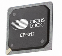
EP9312-CB Cirrus Logic Inc, EP9312-CB Datasheet - Page 526

EP9312-CB
Manufacturer Part Number
EP9312-CB
Description
System-on-Chip Processor
Manufacturer
Cirrus Logic Inc
Series
EP9r
Datasheets
1.EP9307-CRZ.pdf
(824 pages)
2.EP9312-IBZ.pdf
(4 pages)
3.EP9312-CB.pdf
(62 pages)
4.EP9312-CB.pdf
(17 pages)
Specifications of EP9312-CB
Peak Reflow Compatible (260 C)
No
A/d Converter
12 Bits
Leaded Process Compatible
No
No. Of I/o Pins
65
Package / Case
352-BGA
Core Processor
ARM9
Core Size
16/32-Bit
Speed
200MHz
Connectivity
EBI/EMI, EIDE, Ethernet, I²C, IrDA, Keypad/Touchscreen, SPI, UART/USART, USB
Peripherals
AC'97, DMA, I²:S, LCD, LED, MaverickKey, POR, PWM, WDT
Number Of I /o
16
Program Memory Type
ROMless
Ram Size
32K x 8
Voltage - Supply (vcc/vdd)
1.65 V ~ 3.6 V
Data Converters
A/D 8x12b
Oscillator Type
External
Operating Temperature
0°C ~ 70°C
Processor Series
EP93xx
Core
ARM920T
Data Bus Width
32 bit
3rd Party Development Tools
MDK-ARM, RL-ARM, ULINK2
Lead Free Status / RoHS Status
Contains lead / RoHS non-compliant
Eeprom Size
-
Program Memory Size
-
Lead Free Status / Rohs Status
No
Other names
598-1257
Available stocks
Company
Part Number
Manufacturer
Quantity
Price
Part Number:
EP9312-CB
Manufacturer:
CIRRUS
Quantity:
20 000
- EP9307-CRZ PDF datasheet
- EP9312-IBZ PDF datasheet #2
- EP9312-CB PDF datasheet #3
- EP9312-CB PDF datasheet #4
- Current page: 526 of 824
- Download datasheet (13Mb)
14
14-4
UART1 With HDLC and Modem Control Signals
EP93xx User’s Guide
14.2.1.4 Baud Rate Generator
14.2.1.5 Transmit FIFO
14.2.1.6 Receive FIFO
14.2.1.7 Transmit Logic
14.2.1.8 Receive Logic
14.2.1.9 Interrupt Generation Logic
The baud rate generator contains free-running counters which generate the internal x16
clocks and the Baud16 signal. Baud16 provides timing information for UART transmit and
receive control. Baud16 is a stream of pulses with a width of one UARTCLK clock period and
a frequency of sixteen times the baud rate.
The transmit FIFO is an 8-bit wide, 16-entry deep, first-in, first-out memory buffer. CPU data
written across the APB interface and data written across the DMA interface is stored in the
FIFO until read out by the transmit logic. The transmit FIFO can be disabled to act as a one-
byte holding register.
The receive FIFO is an 11 bit wide, 16-entry deep, FIFO memory buffer. Received data, and
corresponding error bits, are stored in the receive FIFO by the receive logic until read out by
the CPU across the APB interface or across the DMA interface. The FIFO can be disabled to
act as a one-byte holding register.
The transmit logic performs parallel-to-serial conversion on the data read from the transmit
FIFO. Control logic outputs the serial bit stream beginning with a start bit, data bits, least
significant bit (LSB) first, followed by parity bit, and then stop bits according to the
programmed configuration in control registers.
The receive logic performs serial-to-parallel conversion on the received bit stream after a
valid start pulse has been detected. Parity, frame error checking and line break detection are
also performed, and the data with associated parity, framing and break error bits is written to
the receive FIFO.
Four individual maskable active HIGH interrupts are generated by the UART, and a combined
interrupt output is also generated as an OR function of the individual interrupt requests.
The single combined UART interrupt (UARTINTR) is routed to the system interrupt controller.
In addition, a separate receive FIFO interrupt UARTRXINTR and a transmit FIFO interrupt
UARTTXINTR are routed to the system interrupt controller. (See
Interrupt Controller” on page 6-1
status signals indicate to the DMA interface when there is room in the transmit FIFO for more
data and when there is data in the receive FIFO.
Copyright 2007 Cirrus Logic
for additional details.) Separate receive and transmit FIFO
Chapter
6,,
“Vectored
DS785UM1
Related parts for EP9312-CB
Image
Part Number
Description
Manufacturer
Datasheet
Request
R

Part Number:
Description:
IC ARM920T MCU 200MHZ 352-PBGA
Manufacturer:
Cirrus Logic Inc
Datasheet:

Part Number:
Description:
IC ARM9 SOC UNIVERSAL 352PBGA
Manufacturer:
Cirrus Logic Inc
Datasheet:

Part Number:
Description:
IC ARM920T MCU 200MHZ 352-PBGA
Manufacturer:
Cirrus Logic Inc
Datasheet:

Part Number:
Description:
IC Universal Platform ARM9 SOC Prcessor
Manufacturer:
Cirrus Logic Inc
Datasheet:

Part Number:
Description:
IC Universal Platform ARM9 SOC Prcessor
Manufacturer:
Cirrus Logic Inc
Datasheet:

Part Number:
Description:
Development Kit
Manufacturer:
Cirrus Logic Inc
Datasheet:

Part Number:
Description:
Development Kit
Manufacturer:
Cirrus Logic Inc
Datasheet:

Part Number:
Description:
High-efficiency PFC + Fluorescent Lamp Driver Reference Design
Manufacturer:
Cirrus Logic Inc
Datasheet:

Part Number:
Description:
Development Kit
Manufacturer:
Cirrus Logic Inc
Datasheet:

Part Number:
Description:
Development Kit
Manufacturer:
Cirrus Logic Inc
Datasheet:

Part Number:
Description:
Development Kit
Manufacturer:
Cirrus Logic Inc
Datasheet:

Part Number:
Description:
Development Kit
Manufacturer:
Cirrus Logic Inc
Datasheet:

Part Number:
Description:
Ref Bd For Speakerbar MSA & DSP Products
Manufacturer:
Cirrus Logic Inc


