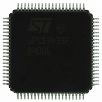
UPSD3433EB40U6 STMicroelectronics, UPSD3433EB40U6 Datasheet - Page 84

UPSD3433EB40U6
Manufacturer Part Number
UPSD3433EB40U6
Description
MCU 8BIT 8032 128KB FLASH 80TQFP
Manufacturer
STMicroelectronics
Series
µPSDr
Datasheet
1.UPSD3434EB40T6.pdf
(293 pages)
Specifications of UPSD3433EB40U6
Core Processor
8032
Core Size
8-Bit
Speed
40MHz
Connectivity
I²C, IrDA, SPI, UART/USART, USB
Peripherals
LVD, POR, PWM, WDT
Number Of I /o
46
Program Memory Size
160KB (160K x 8)
Program Memory Type
FLASH
Ram Size
8K x 8
Voltage - Supply (vcc/vdd)
3 V ~ 5.5 V
Data Converters
A/D 8x10b
Oscillator Type
Internal
Operating Temperature
-40°C ~ 85°C
Package / Case
80-TQFP, 80-VQFP
For Use With
497-5518 - EVAL BOARD RFID READER497-5046 - KIT TOOL FOR ST7/UPSD/STR7 MCU
Lead Free Status / RoHS Status
Lead free / RoHS Compliant
Eeprom Size
-
Other names
497-5660
Available stocks
Company
Part Number
Manufacturer
Quantity
Price
Company:
Part Number:
UPSD3433EB40U6
Manufacturer:
STMicroelectronics
Quantity:
10 000
- Current page: 84 of 293
- Download datasheet (5Mb)
Supervisory functions
19.2
19.3
19.4
19.5
Note:
84/293
Low V
An internal reset is generated by the LVD circuit when V
V
asserted for t
disabled by SFR), even in Idle Mode and Power-down Mode. The LVD input has a voltage
hysteresis of V
Important note: The LVD voltage threshold is V
3.3V V
uPSD34xxV devices, since these supplies are one in the same on the circuit board.
However, for 5V uPSD34xx devices, V
voltage supply (V
case of 5V uPSD34xx devices, an external means is required to monitor the separate 5V
V
Power-up reset
At power up, the internal reset generated by the LVD circuit is latched as a logic '1' in the
POR bit of the SFR named PCON
determine whether the last MCU reset was the result of a power up (cold reset) or a reset
from some other condition (warm reset). This bit must be cleared with software.
JTAG debug reset
The JTAG Debug Unit can generate a reset for debugging purposes. This reset source is
also available when the MCU is in Idle Mode and Power-Down Mode (the user can use the
JTAG debugger to exit these modes).
Watchdog timer, WDT
When enabled, the WDT will generate a reset whenever it overflows. Firmware that is
behaving correctly will periodically clear the WDT before it overflows. Run-away firmware
will not be able to clear the WDT, and a reset will be generated.
By default, the WDT is disabled after each reset.
The WDT is not active during Idle mode or Power-down Mode.
There are two SFRs that control the WDT, they are WDKEY
WDRST
If WDKEY contains 55h, the WDT is disabled. Any value other than 55h in WDKEY will
enable the WDT. By default, after any reset condition, WDKEY is automatically loaded with
55h, disabling the WDT. It is the responsibility of initialization firmware to write some value
other than 55h to WDKEY after each reset if the WDT is to be used.
The WDT consists of a 24-bit up-counter
default after every reset. The most significant byte of this counter is controlled by the SFR,
WDRST. After being enabled by WDKEY, the 24-bit count is increased by 1 for each MCU
machine cycle. When the count overflows beyond FFFFFh (2
reset is issued and the WDT is automatically disabled (WDKEY = 55h again).
LV_THRESH
DD
supply, if desired.
CC
(Table 40 on page
CC
supply on the MCU Module and the 3.3V V
. After V
RST_ACTV
voltage detect, LVD
RST_HYS
LV_THRESH
CC
before it is released. The LVD circuit is always enabled (cannot be
returns to the reset threshold, the MCU_RESET signal will remain
and will reject voltage spikes less than a duration of t
86).
is too low), but good for monitoring the 3.3V V
(Table 26 on page
LV_THRESH
(Figure
LV_THRESH
24), whose initial count is 000000h by
is not suitable for monitoring the 5V V
DD
66). Software can read this bit to
CC
supply on the PSD Module for 3.3V
, suitable for monitoring both the
drops below the reset threshold,
(Table 39 on page
24
MCU machine cycles), a
CC
RST_FIL
supply. In the
86) and
uPSD34xx
.
DD
Related parts for UPSD3433EB40U6
Image
Part Number
Description
Manufacturer
Datasheet
Request
R

Part Number:
Description:
MCU 8BIT 8032 128KB FLASH 80TQFP
Manufacturer:
STMicroelectronics
Datasheet:

Part Number:
Description:
MCU 8BIT 8032 128KB FLASH 52TQFP
Manufacturer:
STMicroelectronics
Datasheet:

Part Number:
Description:
STMicroelectronics [RIPPLE-CARRY BINARY COUNTER/DIVIDERS]
Manufacturer:
STMicroelectronics
Datasheet:

Part Number:
Description:
STMicroelectronics [LIQUID-CRYSTAL DISPLAY DRIVERS]
Manufacturer:
STMicroelectronics
Datasheet:

Part Number:
Description:
BOARD EVAL FOR MEMS SENSORS
Manufacturer:
STMicroelectronics
Datasheet:

Part Number:
Description:
NPN TRANSISTOR POWER MODULE
Manufacturer:
STMicroelectronics
Datasheet:

Part Number:
Description:
TURBOSWITCH ULTRA-FAST HIGH VOLTAGE DIODE
Manufacturer:
STMicroelectronics
Datasheet:

Part Number:
Description:
Manufacturer:
STMicroelectronics
Datasheet:

Part Number:
Description:
DIODE / SCR MODULE
Manufacturer:
STMicroelectronics
Datasheet:

Part Number:
Description:
DIODE / SCR MODULE
Manufacturer:
STMicroelectronics
Datasheet:

Part Number:
Description:
Search -----> STE16N100
Manufacturer:
STMicroelectronics
Datasheet:

Part Number:
Description:
Search ---> STE53NA50
Manufacturer:
STMicroelectronics
Datasheet:


