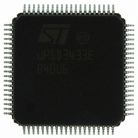
UPSD3433EB40U6 STMicroelectronics, UPSD3433EB40U6 Datasheet - Page 74

UPSD3433EB40U6
Manufacturer Part Number
UPSD3433EB40U6
Description
MCU 8BIT 8032 128KB FLASH 80TQFP
Manufacturer
STMicroelectronics
Series
µPSDr
Datasheet
1.UPSD3434EB40T6.pdf
(293 pages)
Specifications of UPSD3433EB40U6
Core Processor
8032
Core Size
8-Bit
Speed
40MHz
Connectivity
I²C, IrDA, SPI, UART/USART, USB
Peripherals
LVD, POR, PWM, WDT
Number Of I /o
46
Program Memory Size
160KB (160K x 8)
Program Memory Type
FLASH
Ram Size
8K x 8
Voltage - Supply (vcc/vdd)
3 V ~ 5.5 V
Data Converters
A/D 8x10b
Oscillator Type
Internal
Operating Temperature
-40°C ~ 85°C
Package / Case
80-TQFP, 80-VQFP
For Use With
497-5518 - EVAL BOARD RFID READER497-5046 - KIT TOOL FOR ST7/UPSD/STR7 MCU
Lead Free Status / RoHS Status
Lead free / RoHS Compliant
Eeprom Size
-
Other names
497-5660
Available stocks
Company
Part Number
Manufacturer
Quantity
Price
Company:
Part Number:
UPSD3433EB40U6
Manufacturer:
STMicroelectronics
Quantity:
10 000
- Current page: 74 of 293
- Download datasheet (5Mb)
I/O ports of mcu module
Note:
17.1.4
74/293
1
Table 29.
Write '1' or '0' for pin output. Read for pin input, but prior to READ, this bit must have been
set to '1' by firmware or by a reset event.
Alternate Functions
There are five SFRs used to control the mapping of alternate functions onto MCU port pins,
and these SFRs are depicted as switches in
●
●
●
Since these SFRs are cleared by a reset, then by default all port pins function as GPIO (not
the alternate function) until firmware initializes these SFRs.
Each pin on each of the three ports can be independently assigned a different function on a
pin-by-pin basis.
The peripheral functions Timer 2, UART1, and I
1 and Port 4 for additional flexibility by giving a wider choice of peripheral usage on a limited
number of device pins.
When the selected alternate function is UART0, UART1, or SPI, then the related pins are in
quasi-bidirectional mode, including the use of the high-side driver for rapid 0-to-1 output
transitions. The high-side driver is enabled for just one MCU_CLK period on 0-to-1
transitions by the delay function at the “digital_alt_func_data_out” signal pictured in
Figure 17 on page 71
If the alternate function is Timer 0, Timer 1, Timer 2, or PCA input, then the related pins are
in quasi-bidirectional mode, but input only.
If the alternate function is ADC, then for each pin the pull-ups, the high-side driver, and the
low-side driver are disabled. The analog input is routed directly to the ADC unit. Only Port 1
supports analog functions
If the alternate function is I
quasi-bidirectional mode but the high-side driver is not enabled for one cycle when
Bit 7
P4.7
Bit
Port 3 uses the SFR, P3SFS
Port 1 uses SFRs, P1SFS0
Port 4 uses SFRs, P4SFS0
7
6
5
4
3
2
1
0
P4: I/O Port 4 Register (SFR C0h, reset value FFh)
Symbol
Bit 6
P4.6
P4.7
P4.6
P4.5
P4.4
P4.3
P4.2
P4.1
P4.0
through
Bit 5
P4.5
R/W
R,W
R,W
R,W
R,W
R,W
R,W
R,W
R,W
(Figure 17 on page
2
C, the related pins will be in open drain mode, which is just like
Figure 19 on page
(Table 31 on page
(Table 34 on page
(Table 30 on page
Bit 4
P4.4
Figure 16 on page
71). Port 1 is not 5V tolerant.
2
C may be split independently between Port
Bit 3
P4.3
72.
75) and P1SFS1
76) and P4SFS1
75).
Function
Port pin 4.7
Port pin 4.6
Port pin 4.5
Port pin 4.4
Port pin 4.3
Port pin 4.2
Port pin 4.1
Port pin 4.0
Bit 2
P4.2
71.
(1)
(Table 32 on page
(Table 35 on page
Bit 1
P4.1
uPSD34xx
Bit 0
P4.0
76).
76).
Related parts for UPSD3433EB40U6
Image
Part Number
Description
Manufacturer
Datasheet
Request
R

Part Number:
Description:
MCU 8BIT 8032 128KB FLASH 80TQFP
Manufacturer:
STMicroelectronics
Datasheet:

Part Number:
Description:
MCU 8BIT 8032 128KB FLASH 52TQFP
Manufacturer:
STMicroelectronics
Datasheet:

Part Number:
Description:
STMicroelectronics [RIPPLE-CARRY BINARY COUNTER/DIVIDERS]
Manufacturer:
STMicroelectronics
Datasheet:

Part Number:
Description:
STMicroelectronics [LIQUID-CRYSTAL DISPLAY DRIVERS]
Manufacturer:
STMicroelectronics
Datasheet:

Part Number:
Description:
BOARD EVAL FOR MEMS SENSORS
Manufacturer:
STMicroelectronics
Datasheet:

Part Number:
Description:
NPN TRANSISTOR POWER MODULE
Manufacturer:
STMicroelectronics
Datasheet:

Part Number:
Description:
TURBOSWITCH ULTRA-FAST HIGH VOLTAGE DIODE
Manufacturer:
STMicroelectronics
Datasheet:

Part Number:
Description:
Manufacturer:
STMicroelectronics
Datasheet:

Part Number:
Description:
DIODE / SCR MODULE
Manufacturer:
STMicroelectronics
Datasheet:

Part Number:
Description:
DIODE / SCR MODULE
Manufacturer:
STMicroelectronics
Datasheet:

Part Number:
Description:
Search -----> STE16N100
Manufacturer:
STMicroelectronics
Datasheet:

Part Number:
Description:
Search ---> STE53NA50
Manufacturer:
STMicroelectronics
Datasheet:


