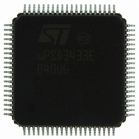
UPSD3433EB40U6 STMicroelectronics, UPSD3433EB40U6 Datasheet - Page 229

UPSD3433EB40U6
Manufacturer Part Number
UPSD3433EB40U6
Description
MCU 8BIT 8032 128KB FLASH 80TQFP
Manufacturer
STMicroelectronics
Series
µPSDr
Datasheet
1.UPSD3434EB40T6.pdf
(293 pages)
Specifications of UPSD3433EB40U6
Core Processor
8032
Core Size
8-Bit
Speed
40MHz
Connectivity
I²C, IrDA, SPI, UART/USART, USB
Peripherals
LVD, POR, PWM, WDT
Number Of I /o
46
Program Memory Size
160KB (160K x 8)
Program Memory Type
FLASH
Ram Size
8K x 8
Voltage - Supply (vcc/vdd)
3 V ~ 5.5 V
Data Converters
A/D 8x10b
Oscillator Type
Internal
Operating Temperature
-40°C ~ 85°C
Package / Case
80-TQFP, 80-VQFP
For Use With
497-5518 - EVAL BOARD RFID READER497-5046 - KIT TOOL FOR ST7/UPSD/STR7 MCU
Lead Free Status / RoHS Status
Lead free / RoHS Compliant
Eeprom Size
-
Other names
497-5660
Available stocks
Company
Part Number
Manufacturer
Quantity
Price
Company:
Part Number:
UPSD3433EB40U6
Manufacturer:
STMicroelectronics
Quantity:
10 000
- Current page: 229 of 293
- Download datasheet (5Mb)
uPSD34xx
Note:
Note:
Note:
Note:
Note:
Note:
1
2
3
1
2
1
2
1
2
3
1
2
3
2
1
Table 126. MCU I/O mode port A data out register
Port A not available on 52-pin uPSD34xx devices
For each bit, 1 = drive port pin to logic '1,' 0 = drive port pin to logic ’0’
Default state of register is 00h after reset or power-up
Table 127. MCU I/O mode port B data out register (address = csiop + offset 05h)
For each bit, 1 = drive port pin to logic '1,' 0 = drive port pin to logic ’0’
Default state of register is 00h after reset or power-up
Table 128. MCU I/O mode port C data out register (address = csiop + offset 12h)
For each bit, 1 = drive port pin to logic '1,' 0 = drive port pin to logic ’0’
Default state of register is 00h after reset or power-up
Table 129. MCU I/O mode port D data out register (address = csiop + offset 13h)
For each bit, 1 = drive port pin to logic '1,' 0 = drive port pin to logic ’0’
Default state for register is 00h after reset or power-up
Not available on 52-pin uPSD34xx devices
Table 130. MCU I/O mode port A direction register
Port A not available on 52-pin uPSD34xx devices
For each bit, 1 = out from uPSD34xx port pin1, 0 = in to PSD34xx port pin
Default state for register is 00h after reset or power-up
Table 131. MCU I/O mode port B direction in register (address = csiop + offset 07h)
For each bit, 1 = out from uPSD34xx port pin1, 0 = in to PSD34xx port pin
Default state for register is 00h after reset or power-up
Bit 7
Bit 7
Bit 7
Bit 7
Bit 7
Bit 7
PC7
PB7
PB7
N/A
PA7
PA7
Bit 6
Bit 6
Bit 6
Bit 6
Bit 6
Bit 6
PB6
PB6
N/A
N/A
PA6
PA6
Bit 5
Bit 5
Bit 5
Bit 5
Bit 5
Bit 5
PB5
PB5
N/A
N/A
PA5
PA5
Bit 4
Bit 4
Bit 4
Bit 4
Bit 4
Bit 4
PC4
PB4
PB4
PA4
PA4
N/A
Bit 3
Bit 3
Bit 3
Bit 3
Bit 3
Bit 3
PC3
PB3
PB3
N/A
PA3
PA3
(1)
(1)
(address = csiop + offset 04h)
(address = csiop + offset 06h)
PD2
Bit 2
Bit 2
Bit 2
Bit 2
Bit 2
Bit 2
PC2
PB2
PB2
PA2
PA2
(3)
Bit 1
Bit 1
Bit 1
Bit 1
Bit 1
Bit 1
PD1
PB1
PB1
N/A
PA1
PA1
PSD module
Bit 0
Bit 0
Bit 0
Bit 0
Bit 0
Bit 0
PB0
PB0
N/A
N/A
229/293
PA0
PA0
Related parts for UPSD3433EB40U6
Image
Part Number
Description
Manufacturer
Datasheet
Request
R

Part Number:
Description:
MCU 8BIT 8032 128KB FLASH 80TQFP
Manufacturer:
STMicroelectronics
Datasheet:

Part Number:
Description:
MCU 8BIT 8032 128KB FLASH 52TQFP
Manufacturer:
STMicroelectronics
Datasheet:

Part Number:
Description:
STMicroelectronics [RIPPLE-CARRY BINARY COUNTER/DIVIDERS]
Manufacturer:
STMicroelectronics
Datasheet:

Part Number:
Description:
STMicroelectronics [LIQUID-CRYSTAL DISPLAY DRIVERS]
Manufacturer:
STMicroelectronics
Datasheet:

Part Number:
Description:
BOARD EVAL FOR MEMS SENSORS
Manufacturer:
STMicroelectronics
Datasheet:

Part Number:
Description:
NPN TRANSISTOR POWER MODULE
Manufacturer:
STMicroelectronics
Datasheet:

Part Number:
Description:
TURBOSWITCH ULTRA-FAST HIGH VOLTAGE DIODE
Manufacturer:
STMicroelectronics
Datasheet:

Part Number:
Description:
Manufacturer:
STMicroelectronics
Datasheet:

Part Number:
Description:
DIODE / SCR MODULE
Manufacturer:
STMicroelectronics
Datasheet:

Part Number:
Description:
DIODE / SCR MODULE
Manufacturer:
STMicroelectronics
Datasheet:

Part Number:
Description:
Search -----> STE16N100
Manufacturer:
STMicroelectronics
Datasheet:

Part Number:
Description:
Search ---> STE53NA50
Manufacturer:
STMicroelectronics
Datasheet:


